ZHCSIJ3C June 2008 – July 2018 ADS7950 , ADS7951 , ADS7952 , ADS7953 , ADS7954 , ADS7955 , ADS7956 , ADS7957 , ADS7958 , ADS7959 , ADS7960 , ADS7961
PRODUCTION DATA.
- 1 特性
- 2 应用
- 3 说明
- 4 修订历史记录
- 5 器件比较表
- 6 Pin Configuration and Functions
-
7 Specifications
- 7.1 Absolute Maximum Ratings
- 7.2 ESD Ratings
- 7.3 Recommended Operating Conditions
- 7.4 Thermal Information: TSSOP
- 7.5 Thermal Information: VQFN
- 7.6 Electrical Characteristics: ADS7950, ADS7951, ADS7952, ADS7953
- 7.7 Electrical Characteristics, ADS7954, ADS7955, ADS7956, ADS7957
- 7.8 Electrical Characteristics, ADS7958, ADS7959, ADS7960, ADS7961
- 7.9 Timing Requirements
- 7.10 Typical Characteristics (All ADS79xx Family Devices)
- 7.11 Typical Characteristics (12-Bit Devices Only)
- 7.12 Typical Characteristics (12-Bit Devices Only)
- 8 Detailed Description
- 9 Application and Implementation
- 10Power Supply Recommendations
- 11Layout
- 12器件和文档支持
- 13机械、封装和可订购信息
封装选项
请参考 PDF 数据表获取器件具体的封装图。
机械数据 (封装 | 引脚)
- RGE|24
- DBT|30
散热焊盘机械数据 (封装 | 引脚)
- RGE|24
订购信息
7.9 Timing Requirements
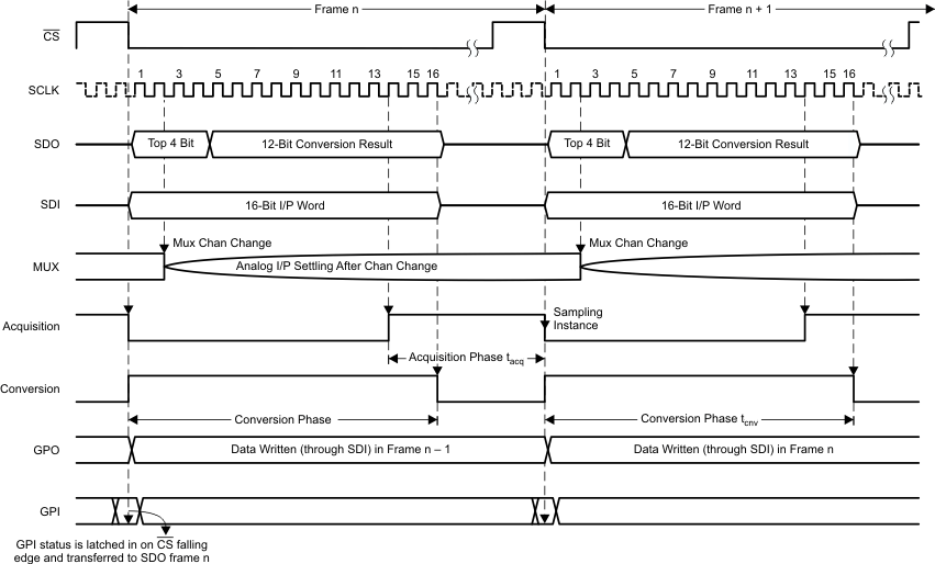
All specifications typical at –40°C to 125°C, +VA = 2.7 V to 5.25 V (unless otherwise specified)(1)(2) (see Figure 1, Figure 2, Figure 3, and Figure 4)(1) 1.8V specifications apply from 1.7 V to 1.9 V, 3 V specifications apply from 2.7 V to 3.6 V, 5 V specifications apply from 4.75 V to 5.25 V.
(2) With 50-pF load
 Figure 1. Device Operation Timing Diagram
  Figure 2. Serial Interface Timing Diagram for 12-Bit Devices (ADS7950/51/52/53)
  Figure 3. Serial Interface Timing Diagram for 10-Bit Devices (ADS7954/55/56/57)
  Figure 4. Serial Interface Timing Diagram for 8-Bit Devices (ADS7958/59/60/61)