ZHCSIJ3C June   2008  – July 2018 ADS7950 , ADS7951 , ADS7952 , ADS7953 , ADS7954 , ADS7955 , ADS7956 , ADS7957 , ADS7958 , ADS7959 , ADS7960 , ADS7961

PRODUCTION DATA.  

  1. 特性
  2. 应用
    1.     详细方框图
  3. 说明
  4. 修订历史记录
  5. 器件比较表
  6. Pin Configuration and Functions
    1.     Pin Functions: TSSOP Packages
    2.     Pin Functions: VQFN Packages
  7. Specifications
    1. 7.1  Absolute Maximum Ratings
    2. 7.2  ESD Ratings
    3. 7.3  Recommended Operating Conditions
    4. 7.4  Thermal Information: TSSOP
    5. 7.5  Thermal Information: VQFN
    6. 7.6  Electrical Characteristics: ADS7950, ADS7951, ADS7952, ADS7953
    7. 7.7  Electrical Characteristics, ADS7954, ADS7955, ADS7956, ADS7957
    8. 7.8  Electrical Characteristics, ADS7958, ADS7959, ADS7960, ADS7961
    9. 7.9  Timing Requirements
    10. 7.10 Typical Characteristics (All ADS79xx Family Devices)
    11. 7.11 Typical Characteristics (12-Bit Devices Only)
    12. 7.12 Typical Characteristics (12-Bit Devices Only)
  8. Detailed Description
    1. 8.1 Overview
    2. 8.2 Functional Block Diagram
    3. 8.3 Feature Description
      1. 8.3.1 Reference
      2. 8.3.2 Power Saving
    4. 8.4 Device Functional Modes
      1. 8.4.1 Channel Sequencing Modes
      2. 8.4.2 Device Programming and Mode Control
        1. 8.4.2.1 Mode Control Register
        2. 8.4.2.2 Program Registers
      3. 8.4.3 Device Power-Up Sequence
      4. 8.4.4 Operating in Manual Mode
      5. 8.4.5 Operating in Auto-1 Mode
      6. 8.4.6 Operating in Auto-2 Mode
      7. 8.4.7 Continued Operation in a Selected Mode
    5. 8.5 Programming
      1. 8.5.1 Digital Output
      2. 8.5.2 GPIO Registers
      3. 8.5.3 Alarm Thresholds for GPIO Pins
  9. Application and Implementation
    1. 9.1 Application Information
      1. 9.1.1 Analog Input
    2. 9.2 Typical Applications
      1. 9.2.1 Unbuffered Multiplexer Output (MXO)
        1. 9.2.1.1 Design Requirements
        2. 9.2.1.2 Detailed Design Procedure
        3. 9.2.1.3 Application Curves
      2. 9.2.2 OPA192 Buffered Multiplexer Output (MXO)
        1. 9.2.2.1 Design Requirements
        2. 9.2.2.2 Detailed Design Procedure
        3. 9.2.2.3 Application Curves
  10. 10Power Supply Recommendations
  11. 11Layout
    1. 11.1 Layout Guidelines
    2. 11.2 Layout Examples
  12. 12器件和文档支持
    1. 12.1 文档支持
      1. 12.1.1 相关文档
    2. 12.2 相关链接
    3. 12.3 接收文档更新通知
    4. 12.4 社区资源
    5. 12.5 商标
    6. 12.6 静电放电警告
    7. 12.7 术语表
  13. 13机械、封装和可订购信息

封装选项

请参考 PDF 数据表获取器件具体的封装图。

机械数据 (封装 | 引脚)
  • RGE|24
  • DBT|30
散热焊盘机械数据 (封装 | 引脚)
订购信息

Device Power-Up Sequence

The device power-up sequence is shown in Figure 49. By default, the Mode Control Register is configured for manual mode and the default channel is channel 0. As explained previously, these devices offer Program Registers to configure user programmable features like GPIOs, Alarms, and to pre-program the channel sequence for Auto modes. At ‘power up or on reset’ these registers are set to the default values listed in Table 1 to Table 11. On power up or after reset It is required to program Mode Control Register and Program Register to required mode of operation. Once configured; the device is ready to use in any of the three channel sequencing modes namely Manual, Auto-1, and Auto-2.
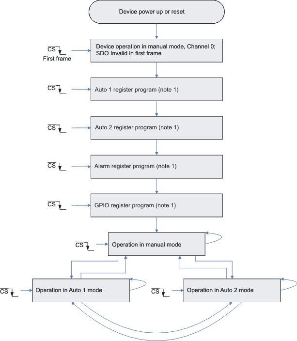
ADS7950 ADS7951 ADS7952 ADS7953 ADS7954 ADS7955 ADS7956 ADS7957 ADS7958 ADS7959 ADS7960 ADS7961 dev_pwr_up_las605.gif
The device continues its operation in manual mode channel 0 throughout the programming sequence and outputs valid conversion results. It is possible to change channel, range, GPIO by inserting extra frames in between two programming blocks. It is also possible to bypass any programming block if the user does not intend to use that feature.
It is possible to reprogram the device at any time during operation, regardless of what mode the device is in. During programming the device continues its operation in whatever mode it is in and outputs valid data.
Figure 49. Device Power-Up Sequence