ZHCSIJ3C June 2008 – July 2018 ADS7950 , ADS7951 , ADS7952 , ADS7953 , ADS7954 , ADS7955 , ADS7956 , ADS7957 , ADS7958 , ADS7959 , ADS7960 , ADS7961
PRODUCTION DATA.
- 1 特性
- 2 应用
- 3 说明
- 4 修订历史记录
- 5 器件比较表
- 6 Pin Configuration and Functions
-
7 Specifications
- 7.1 Absolute Maximum Ratings
- 7.2 ESD Ratings
- 7.3 Recommended Operating Conditions
- 7.4 Thermal Information: TSSOP
- 7.5 Thermal Information: VQFN
- 7.6 Electrical Characteristics: ADS7950, ADS7951, ADS7952, ADS7953
- 7.7 Electrical Characteristics, ADS7954, ADS7955, ADS7956, ADS7957
- 7.8 Electrical Characteristics, ADS7958, ADS7959, ADS7960, ADS7961
- 7.9 Timing Requirements
- 7.10 Typical Characteristics (All ADS79xx Family Devices)
- 7.11 Typical Characteristics (12-Bit Devices Only)
- 7.12 Typical Characteristics (12-Bit Devices Only)
- 8 Detailed Description
- 9 Application and Implementation
- 10Power Supply Recommendations
- 11Layout
- 12器件和文档支持
- 13机械、封装和可订购信息
封装选项
请参考 PDF 数据表获取器件具体的封装图。
机械数据 (封装 | 引脚)
- RGE|24
- DBT|30
散热焊盘机械数据 (封装 | 引脚)
- RGE|24
订购信息
8.4.4 Operating in Manual Mode
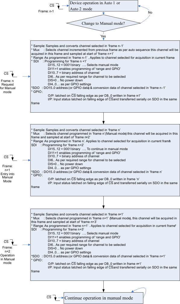
The flowchart in Figure 50 illustrates the steps involved in operating in manual channel sequencing mode. Table 1 lists the mode control register settings for manual mode. There are no program registers in manual mode.
 Figure 50. Entering and Running in Manual Channel Sequencing Mode
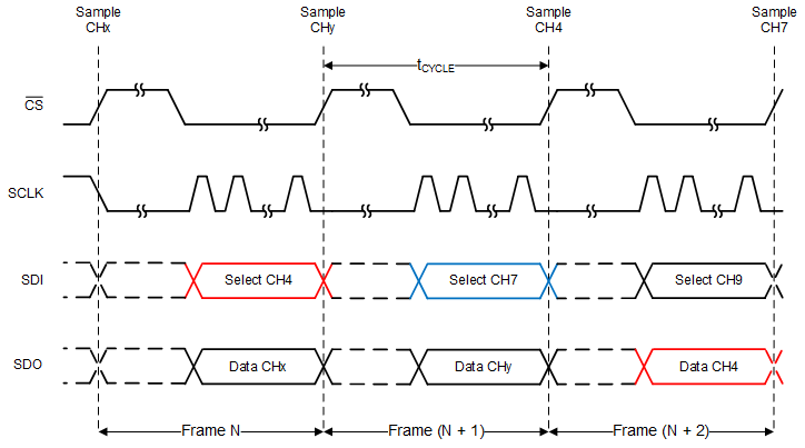
 Figure 51 shows an example in which manual mode is used to scan channels 4, 7, and 9. The command to select channel 4 (CH4) is issued in the Nth frame and the data corresponding to CH4 is available in the (N + 2)th frame. Internally, the SDI command is parsed and on the rising edge of CS of the (N+1)th frame and the MUX switches accordingly on the second falling edge of SCLK in this frame. On the rising edge of CS of the (N+2)th frame, the input signal for CH4 is sampled and the ADC sends the conversion data in this third frame. The device follows the same steps and the ADC sends the conversion data for CH7 and CH9 in the subsequent two frames.
 Figure 51. Example Manual Mode Timing Diagram
 Table 1. Mode Control Register Settings for Manual Mode
| BITS | RESET STATE | LOGIC STATE | FUNCTION | |||
|---|---|---|---|---|---|---|
| DI15-12 | 0001 | 0001 | Selects Manual Mode | |||
| DI11 | 0 | 1 | Enables programming of bits DI06-00. | |||
| 0 | Device retains values of DI06-00 from the previous frame. | |||||
| DI10-07 | 0000 | This four bit data represents the address of the next channel to be selected in the next frame. DI10: MSB and DI07: LSB. For example, 0000 represents channel- 0, 0001 represents channel-1 and so forth. | ||||
| DI06 | 0 | 0 | Selects 0 to VREF input range (Range 1) | |||
| 1 | Selects 0 to 2xVREF input range (Range 2) | |||||
| DI05 | 0 | 0 | Device normal operation (no powerdown) | |||
| 1 | Device powers down on 16th SCLK falling edge | |||||
| DI04 | 0 | 0 | SDO outputs current channel address of the channel on DO15..12 followed by 12 bit conversion result on DO11..00. | |||
| 1 | GPIO3-GPIO0 data (both input and output) is mapped onto DO15-DO12 in the order shown below. Lower data bits DO11-DO00 represent 12-bit conversion result of the current channel. | |||||
| DOI5 | DOI4 | DOI3 | DOI2 | |||
| GPIO3(1) | GPIO2(1) | GPIO1(1) | GPIO0(1) | |||
| DI03-00 | 0000 | GPIO data for the channels configured as output. Device will ignore the data for the channel which is configured as input. SDI bit and corresponding GPIO information is given below | ||||
| DI03 | DI02 | DI01 | DI00 | |||
| GPIO3(1) | GPIO2(1) | GPIO1(1) | GPIO0(1) | |||