ZHCSIK6D November 2017 – June 2024 ADS8166 , ADS8167 , ADS8168
PRODUCTION DATA
- 1
- 1 特性
- 2 应用
- 3 说明
- 4 Pin Configuration and Functions
- 5 Specifications
- 6 Detailed Description
-
7 Register Maps
- 7.1
Interface and Hardware Configuration Registers
- 7.1.1 REG_ACCESS Register (address = 00h) [reset = 00h]
- 7.1.2 PD_CNTL Register (address = 04h) [reset = 00h]
- 7.1.3 SDI_CNTL Register (address = 008h) [reset = 00h]
- 7.1.4 SDO_CNTL1 Register (address = 0Ch) [reset = 00h]
- 7.1.5 SDO_CNTL2 Register (address = 0Dh) [reset = 00h]
- 7.1.6 SDO_CNTL3 Register (address = 0Eh) [reset = 00h]
- 7.1.7 SDO_CNTL4 Register (address = 0Fh) [reset = 00h]
- 7.1.8 DATA_CNTL Register (address = 10h) [reset = 00h]
- 7.1.9 PARITY_CNTL Register (address = 11h) [reset = 00h]
- 7.2 Device Calibration Registers
- 7.3 Analog Input Configuration Registers
- 7.4
Channel Sequence Configuration Registers Map
- 7.4.1 DEVICE_CFG Register (address = 1Ch) [reset = 00h]
- 7.4.2 CHANNEL_ID Register (address = 1Dh) [reset = 00h]
- 7.4.3 SEQ_START Register (address = 1Eh) [reset = 00h]
- 7.4.4 SEQ_ABORT Register (address = 1Fh) [reset = 00h]
- 7.4.5 ON_THE_FLY_CFG Register (address = 2Ah) [reset = 00h]
- 7.4.6 AUTO_SEQ_CFG1 Register (address = 80h) [reset = 00h]
- 7.4.7 AUTO_SEQ_CFG2 Register (address = 82h) [reset = 00h]
- 7.4.8
Custom Channel Sequencing Mode Registers
- 7.4.8.1 CCS_START_INDEX Register (address = 88h) [reset = 00h]
- 7.4.8.2 CCS_END_INDEX Register (address = 89h) [reset = 00h]
- 7.4.8.3 CCS_SEQ_LOOP Register (address = 8Ah) [reset = 00h]
- 7.4.8.4 CCS_CHID_INDEX_m Registers (address = 8C, 8E, 90, 92, 94, 96, 98, 9A, 9C, 9E, A0, A2, A4, A6, A8, and AAh) [reset = 00h]
- 7.4.8.5 REPEAT_INDEX_m Registers (address = 8D, 8F, 91, 93, 95, 97, 99, 9B, 9D, 9F, A1, A3, A5, A7, A9, and ABh) [reset = 00h]
- 7.5
Digital Window Comparator Configuration Registers Map
- 7.5.1 ALERT_CFG Register (address = 2Eh) [reset = 00h]
- 7.5.2 HI_TRIG_AINx[15:0] Register (address = 4Dh to 30h) [reset = 0000h]
- 7.5.3 LO_TRIG_AINx[15:0] Register (address = 71h to 54h) [reset = 0000h]
- 7.5.4 HYSTERESIS_AINx[7:0] Register (address = 4Fh to 33h) [reset = 00h]
- 7.5.5 ALERT_LO_STATUS Register (address = 78h) [reset = 00h]
- 7.5.6 ALERT_HI_STATUS Register (address = 79h) [reset = 00h]
- 7.5.7 ALERT_STATUS Register (address = 7Ah) [reset = 00h]
- 7.5.8 CURR_ALERT_LO_STATUS Register (address = 7Ch) [reset = 00h]
- 7.5.9 CURR_ALERT_HI_STATUS Register (address = 7Dh) [reset = 00h]
- 7.5.10 CURR_ALERT_STATUS Register (address = 7Eh) [reset = 00h]
- 7.1
Interface and Hardware Configuration Registers
- 8 Application and Implementation
- 9 Device and Documentation Support
- 10Revision History
- 11Mechanical, Packaging, and Orderable Information
Abstract
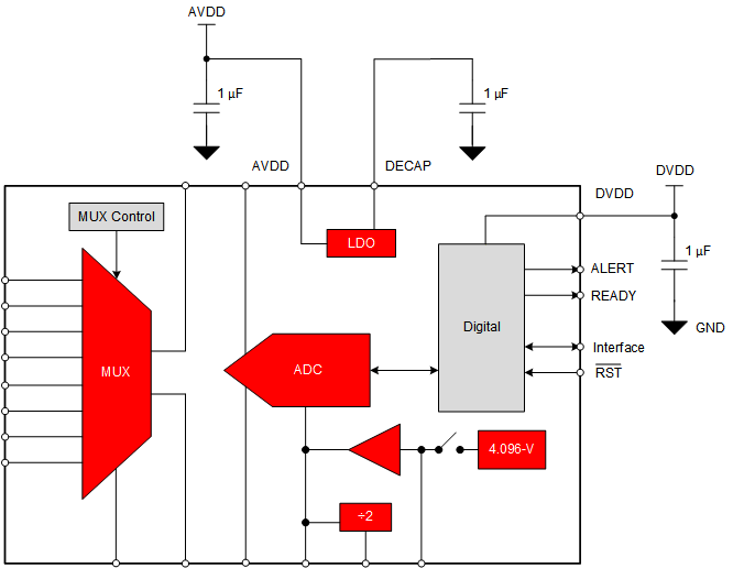
The ADS816x has two separate power supplies: AVDD and DVDD. The internal reference, reference buffer, multiplexer, and the internal LDO operate on AVDD. The ADC core operates on the LDO output (available on the DECAP pin). DVDD is used for setting the logic levels on the digital interface. AVDD and DVDD are independently set to any value within the permissible ranges. During normal operation, if any voltage on the AVDD supply drops below the AVDD minimum specification, then ramp the AVDD supply down to ≤ 0.7V before power-up. Also during power-up, make sure AVDD monotonously rises to the desired operating voltage above the minimum AVDD specification.
When using an internal reference, set AVDD so that 4.5V ≤ AVDD ≤ 5.5V.
The AVDD supply voltage value defines the permissible range for the external reference voltage, VREF, on the REFIO pin. To use the external reference voltage (VREF), set AVDD such that 3V ≤ AVDD ≤ (AVDD + 0.3)V.
As shown in Figure 8-6, place a minimum 1µF decoupling capacitor between the AVDD and GND pins and between the DVDD and GND pins. Use a minimum 1µF decoupling capacitor between the DECAP and GND pins.
There are no specific requirements with regard to the power-supply sequencing of the device. However, issue a reset after the supplies are powered and stable to make sure the device is properly configured.
 Figure 8-6 Power-Supply Decoupling