ZHCSCC6D May 2013 – March 2018 ADS7250 , ADS7850 , ADS8350
PRODUCTION DATA.
- 1 特性
- 2 应用范围
- 3 说明
- 4 修订历史记录
- 5 Pin Configuration and Functions
-
6 Specifications
- 6.1 Absolute Maximum Ratings
- 6.2 ESD Ratings
- 6.3 Recommended Operating Conditions
- 6.4 Thermal Information
- 6.5 Electrical Characteristics: All Devices
- 6.6 Electrical Characteristics: ADS7250
- 6.7 Electrical Characteristics: ADS7850
- 6.8 Electrical Characteristics: ADS8350
- 6.9 Timing Requirements
- 6.10 Switching Characteristics
- 6.11 Typical Characteristics: ADS7250
- 6.12 Typical Characteristics: ADS7850
- 6.13 Typical Characteristics: ADS8350
- 6.14 Typical Characteristics: All Devices
- 7 Detailed Description
- 8 Application and Implementation
- 9 Power Supply Recommendations
- 10Layout
- 11器件和文档支持
- 12机械、封装和可订购信息
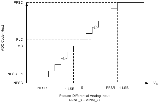
7.3.3 ADC Transfer Function
The device output is in binary twos complement format. Device resolution is calculated by Equation 6:
Equation 6. 1 LSB = (FSR_ADC_x) / (2N)
where
- FSR_ADC_x = 2 x VREFIN_x and
- N is the resolution of the ADC : N = 16 for the ADS8350, N = 14 for the ADS7850, and N = 12 for the ADS7250
Table 1 shows the different input voltages and the corresponding device output codes.
Table 1. Transfer Characteristics
| INPUT VOLTAGE
(AINM_x) |
INPUT VOLTAGE
(AINP_x) |
PSEUDO-DIFFERENTIAL INPUT TO ADC
(AINP_x - AINM_x) |
OUTPUT CODE (HEX) | ||||
|---|---|---|---|---|---|---|---|
| CODE | ADS7250 | ADS7850 | ADS8350 | ||||
| VREFIN_x | 0 | –VREFIN_x | NFSR | NFSC | 800 | 2000 | 8000 |
| 1 LSB | – VREFIN_x + 1 LSB | NFSR + 1 LSB | NFSC + 1 | 801 | 2001 | 8001 | |
| VREFIN_x – 1 LSB | –1 LSB | –1 LSB | MC | FFF | 3FFF | FFFF | |
| VREFIN_x | 0 | 0 | PLC | 000 | 0000 | 0000 | |
| 2 × VREFIN_x – 1 LSB | VREFIN_x – 1 LSB | PFSR – 1 LSB | PFSC | 7FF | 1FFF | 7FFF | |
Figure 51 shows the ideal transfer characteristics for the device.
 Figure 51. Ideal Transfer Characteristics