ZHCSJ89B January   2019  – July 2022 ADS8353-Q1

PRODUCTION DATA  

  1. 1特性
  2. 2应用
  3. 3说明
  4. 4Revision History
  5. 5Pin Configuration and Functions
  6. 6Specifications
    1. 6.1 Absolute Maximum Ratings
    2. 6.2 ESD Ratings
    3. 6.3 Thermal Information
    4. 6.4 Recommended Operating Conditions
    5. 6.5 Electrical Characteristics
    6. 6.6 Timing Requirements
    7. 6.7 Switching Characteristics
    8. 6.8 Timing Diagram
    9. 6.9 Typical Characteristics
  7. 7Detailed Description
    1. 7.1 Overview
    2. 7.2 Functional Block Diagram
    3. 7.3 Feature Description
      1. 7.3.1 Reference
      2. 7.3.2 Analog Inputs
        1. 7.3.2.1 Analog Input: Full-Scale Range Selection
        2. 7.3.2.2 Analog Input: Single-Ended and Pseudo-Differential Configurations
      3. 7.3.3 Transfer Function
    4. 7.4 Device Functional Modes
    5. 7.5 Programming
      1. 7.5.1 Serial Interface
      2. 7.5.2 Write to User-Programmable Registers
      3. 7.5.3 Data Read Operation
        1. 7.5.3.1 Reading User-Programmable Registers
        2. 7.5.3.2 Conversion Data Read
          1. 7.5.3.2.1 32-CLK, Dual-SDO Mode (CFR.B11 = 0, CFR.B10 = 0, Default)
          2. 7.5.3.2.2 32-CLK, Single-SDO Mode (CFR.B11 = 0, CFR.B10 = 1)
      4. 7.5.4 Low-Power Modes
        1. 7.5.4.1 STANDBY Mode
        2. 7.5.4.2 Software Power-Down (SPD) Mode
      5. 7.5.5 Frame Abort, Reconversion, or Short-Cycling
    6. 7.6 Register Maps
      1. 7.6.1 ADS8353-Q1 Registers
  8. 8Application and Implementation
    1. 8.1 Application Information
      1. 8.1.1 Input Amplifier Selection
      2. 8.1.2 Charge Kickback Filter
    2. 8.2 Typical Application
      1. 8.2.1 Design Requirements
      2. 8.2.2 Detailed Design Procedure
      3. 8.2.3 Application Curve
    3. 8.3 Power Supply Recommendations
    4. 8.4 Layout
      1. 8.4.1 Layout Guidelines
      2. 8.4.2 Layout Example
  9. 9Device and Documentation Support
    1. 9.1 Device Support
      1. 9.1.1 Development Support
    2. 9.2 Documentation Support
      1. 9.2.1 Related Documentation
    3. 9.3 接收文档更新通知
    4. 9.4 支持资源
    5. 9.5 Trademarks
    6. 9.6 Electrostatic Discharge Caution
    7. 9.7 术语表
      1.      Mechanical, Packaging, and Orderable Information

封装选项

机械数据 (封装 | 引脚)
散热焊盘机械数据 (封装 | 引脚)
订购信息

Typical Application

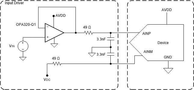
GUID-3064A9EF-D955-4368-8C51-430553905303-low.gif
Only one ADC channel is shown in this diagram. Replicate the same circuit for other ADC channels.
Figure 8-2 DAQ Circuit: Maximum SINAD for a 10-kHz Input Signal at Full Throughput, 32-CLK Interface
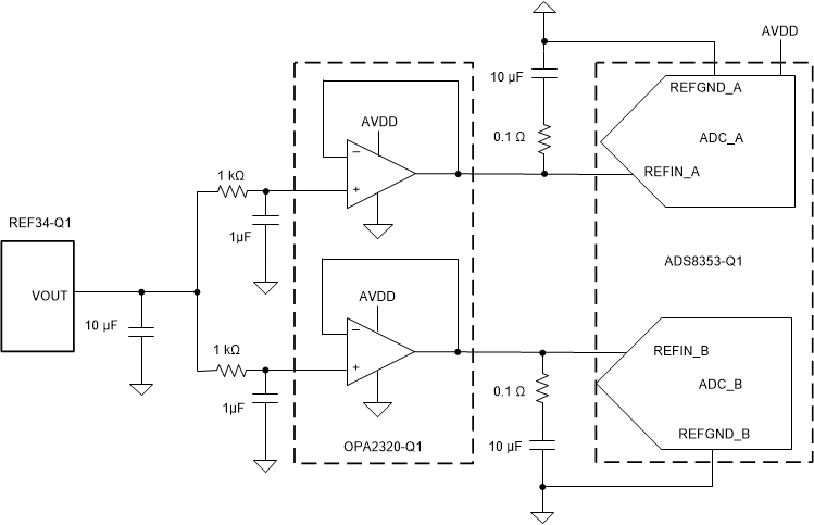
GUID-E29BC8EC-234E-425D-96CE-C2E6134A795C-low.gifFigure 8-3 Reference Drive Circuit