ZHCSJ89B January   2019  – July 2022 ADS8353-Q1

PRODUCTION DATA  

  1. 1特性
  2. 2应用
  3. 3说明
  4. 4Revision History
  5. 5Pin Configuration and Functions
  6. 6Specifications
    1. 6.1 Absolute Maximum Ratings
    2. 6.2 ESD Ratings
    3. 6.3 Thermal Information
    4. 6.4 Recommended Operating Conditions
    5. 6.5 Electrical Characteristics
    6. 6.6 Timing Requirements
    7. 6.7 Switching Characteristics
    8. 6.8 Timing Diagram
    9. 6.9 Typical Characteristics
  7. 7Detailed Description
    1. 7.1 Overview
    2. 7.2 Functional Block Diagram
    3. 7.3 Feature Description
      1. 7.3.1 Reference
      2. 7.3.2 Analog Inputs
        1. 7.3.2.1 Analog Input: Full-Scale Range Selection
        2. 7.3.2.2 Analog Input: Single-Ended and Pseudo-Differential Configurations
      3. 7.3.3 Transfer Function
    4. 7.4 Device Functional Modes
    5. 7.5 Programming
      1. 7.5.1 Serial Interface
      2. 7.5.2 Write to User-Programmable Registers
      3. 7.5.3 Data Read Operation
        1. 7.5.3.1 Reading User-Programmable Registers
        2. 7.5.3.2 Conversion Data Read
          1. 7.5.3.2.1 32-CLK, Dual-SDO Mode (CFR.B11 = 0, CFR.B10 = 0, Default)
          2. 7.5.3.2.2 32-CLK, Single-SDO Mode (CFR.B11 = 0, CFR.B10 = 1)
      4. 7.5.4 Low-Power Modes
        1. 7.5.4.1 STANDBY Mode
        2. 7.5.4.2 Software Power-Down (SPD) Mode
      5. 7.5.5 Frame Abort, Reconversion, or Short-Cycling
    6. 7.6 Register Maps
      1. 7.6.1 ADS8353-Q1 Registers
  8. 8Application and Implementation
    1. 8.1 Application Information
      1. 8.1.1 Input Amplifier Selection
      2. 8.1.2 Charge Kickback Filter
    2. 8.2 Typical Application
      1. 8.2.1 Design Requirements
      2. 8.2.2 Detailed Design Procedure
      3. 8.2.3 Application Curve
    3. 8.3 Power Supply Recommendations
    4. 8.4 Layout
      1. 8.4.1 Layout Guidelines
      2. 8.4.2 Layout Example
  9. 9Device and Documentation Support
    1. 9.1 Device Support
      1. 9.1.1 Development Support
    2. 9.2 Documentation Support
      1. 9.2.1 Related Documentation
    3. 9.3 接收文档更新通知
    4. 9.4 支持资源
    5. 9.5 Trademarks
    6. 9.6 Electrostatic Discharge Caution
    7. 9.7 术语表
      1.      Mechanical, Packaging, and Orderable Information

封装选项

机械数据 (封装 | 引脚)
散热焊盘机械数据 (封装 | 引脚)
订购信息

Pin Configuration and Functions

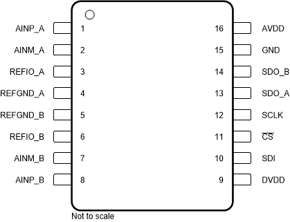
GUID-EB5851CD-8D2A-42CC-93EE-44ACF40DED75-low.gif Figure 5-1 PW Package,16-Pin TSSOP(Top View)
Table 5-1 Pin Functions
PIN TYPE DESCRIPTION
NAME TSSOP
AINM_A 2 Analog input Negative analog input, channel A
AINM_B 7 Analog input Negative analog input, channel B
AINP_A 1 Analog input Positive analog input, channel A
AINP_B 8 Analog input Positive analog input, channel B
AVDD 16 Supply Supply voltage for ADC operation
CS 11 Digital input Chip-select signal; active low
DVDD 9 Digital I/O supply Digital I/O supply
GND 15 Supply Digital ground
REFGND_A 4 Supply Reference ground potential A
REFGND_B 5 Supply Reference ground potential B
REFIO_A 3 Analog input/output Reference voltage input/output, channel A
REFIO_B 6 Analog input/output Reference voltage input/output, channel B
SCLK 12 Digital input Clock for serial communication
SDI 10 Digital input Data input for serial communication
SDO_A 13 Digital output Data output for serial communication, channel A and channel B
SDO_B 14 Digital output Data output for serial communication, channel B