ZHCSKR7A February 2020 – February 2020 ADS8355
PRODUCTION DATA.
- 1 特性
- 2 应用
- 3 说明
- 4 修订历史记录
- 5 Pin Configuration and Functions
- 6 Specifications
-
7 Detailed Description
- 7.1 Overview
- 7.2 Functional Block Diagram
- 7.3 Feature Description
- 7.4 Device Functional Modes
- 7.5 Programming
- 7.6
Register Map
- 7.6.1
ADS8355 Registers
- 7.6.1.1 PD_STANDBY Register (Offset = 4h) [reset = 0h]
- 7.6.1.2 PD_KEY Register (Offset = 5h) [reset = 0h]
- 7.6.1.3 SDO_CTRL Register (Offset = Dh) [reset = 0h]
- 7.6.1.4 DATA_OUT_CTRL Register (Offset = 11h) [reset = 0h]
- 7.6.1.5 REF_SEL Register (Offset = 20h) [reset = 0h]
- 7.6.1.6 REFDAC_A_LSB Register (Offset = 24h) [reset = 0h]
- 7.6.1.7 REFDAC_A_MSB Register (Offset = 25h) [reset = 0h]
- 7.6.1.8 REFDAC_B_LSB Register (Offset = 26h) [reset = 0h]
- 7.6.1.9 REFDAC_B_MSB Register (Offset = 27h) [reset = 0h]
- 7.6.1.10 INPUT_CONFIG Register (Offset = 28h) [reset = 0h]
- 7.6.1
ADS8355 Registers
- 8 Application and Implementation
- 9 Power Supply Recommendations
- 10Layout
- 11器件和文档支持
- 12机械、封装和可订购信息
7.3.3 Transfer Function
The device supports two input configurations:
- Default, single-ended inputs, INPUT_CONFIG register bit 0 = 0
- Pseudo-differential inputs, INPUT_CONFIG register bit 0 = 1
The device supports two output data formats:
- Default, straight binary output, DATA_OUT_CTRL register bit 0 = 0
- Two's compliment output, DATA_OUT_CTRL register bit 0 = 1
Equation 5 calculates the device resolution:
Equation 5. 1 LSB = (FSR_ADC_x) / (2N)
where
- N = 16 and
- FSR_ADC_x is the full-scale input range of the ADC
Table 4 and Table 5 show the different input voltages and the corresponding output codes from the device.
Table 4. Transfer Characteristics for Straight Binary Output (Default)
| INPUT CONFIGURATION | INPUT VOLTAGE | OUTPUT CODE (Hex) | |||
|---|---|---|---|---|---|
| STRAIGHT BINARY | |||||
| AINP_x | AINM_x | AINP_x - AINM_x | CODE | ADS8355 | |
| Single-ended | ≤ 1 LSB | 0 | ≤ 1 LSB | ZC | 0000 |
| FSR_ADC_x / 2 | FSR_ADC_x / 2 | MC | 7FFF | ||
| ≥ FSR_ADC_x – 1 LSB | ≥ FSR_ADC_x – 1 LSB | FSC | FFFF | ||
| Pseudo-differential | ≤ 1 LSB | FSR_ADC_x / 2 | ≤ –FSR_ADC_x / 2 + 1 LSB | ZC | 0000 |
| FSR_ADC_x / 2 | 0 | MC | 7FFF | ||
| ≥ FSR_ADC_x – 1 LSB | ≥ FSR_ADC_x / 2 – 1 LSB | FSC | FFFF | ||
Table 5. Transfer Characteristics for Twos Compliment Output
| INPUT CONFIGURATION | INPUT VOLTAGE | OUTPUT CODE (Hex) | |||
|---|---|---|---|---|---|
| TWO'S COMPLIMENT | |||||
| AINP_x | AINM_x | AINP_x - AINM_x | CODE | ADS8355 | |
| Single-ended | ≤ 1 LSB | 0 | ≤ 1 LSB | NFSC | 8000 |
| FSR_ADC_x / 2 | FSR_ADC_x / 2 | MC | 0000 | ||
| ≥ FSR_ADC_x – 1 LSB | ≥ FSR_ADC_x – 1 LSB | PFSC | 7FFF | ||
| Pseudo-differential | ≤ 1 LSB | FSR_ADC_x / 2 | ≤ –FSR_ADC_x / 2 + 1 LSB | NFSC | 8000 |
| FSR_ADC_x / 2 | 0 | MC | 0000 | ||
| ≥ FSR_ADC_x – 1 LSB | ≥ FSR_ADC_x / 2 – 1 LSB | PFSC | 7FFF | ||
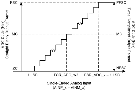
Figure 27 shows the ideal device transfer characteristics for the single-ended analog input.

Figure 27. Ideal Transfer Characteristics for a Single-Ended Analog Input
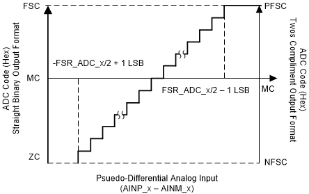
Figure 28 shows the ideal device transfer characteristics for the pseudo-differential analog input.
 Figure 28. Ideal Transfer Characteristics for a Pseudo-Differential Analog Input