SBAS523D October 2010 – September 2017 ADS7223 , ADS7263 , ADS8363
PRODUCTION DATA.
- 1 Features
- 2 Applications
- 3 Description
- 4 Revision History
- 5 Device Comparison Table
- 6 Pin Configuration and Functions
-
7 Specifications
- 7.1 Absolute Maximum Ratings
- 7.2 ESD Ratings
- 7.3 Recommended Operating Conditions
- 7.4 Thermal Information
- 7.5 Electrical Characteristics: General
- 7.6 Electrical Characteristics: ADS8363
- 7.7 Electrical Characteristics: ADS7263
- 7.8 Electrical Characteristics: ADS7223
- 7.9 Switching Characteristics
- 7.10 Typical Characteristics
- 8 Detailed Description
- 9 Application and Implementation
- 10Power Supply Recommendations
- 11Layout
- 12Device and Documentation Support
- 13Mechanical, Packaging, and Orderable Information
11 Layout
11.1 Layout Guidelines
For optimum performance, care must be taken with the physical layout of the ADS8363, ADS7263, and ADS7223 circuitry, particularly if the device is used at the maximum throughput rate. In this case, a fixed phase relationship is recommended between CLOCK and CONVST.
Additionally, the high-performance SAR architecture is sensitive to glitches or sudden changes on the power supply, reference, ground connections, and digital inputs that occur just before latching the output of the internal analog comparator. Therefore, during an operation of an n-bit SAR converter, there are n windows in which large external transient voltages (glitches) can affect the conversion result. Such glitches can originate from switching power supplies, nearby digital logic, or high-power devices. The degree of impact depends on the reference voltage, layout, and the actual timing of the external event.
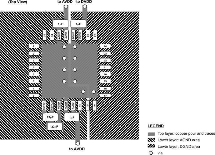
With this possibility in mind, power to the device must be clean and well-bypassed. A 1-µF ceramic bypass capacitor must be placed at each supply pin (connected to the corresponding ground pin) as close to the device as possible.
If the reference voltage is external, the operational amplifier must be able to drive the 22-µF capacitor without oscillation. A series resistor between the driver output and the capacitor may be required. To minimize any code-dependent voltage drop on this path, a small value must be used for this resistor (10 Ω max). TI's REF50xx family is able to directly drive such a capacitive load.
11.1.1 Grounding
The AGND, RGND, and DGND pins must be connected to a clean ground reference. All connections must be kept as short as possible to minimize the inductance of these paths. Using vias connecting the pads directly to the ground plane is recommended. In designs without ground planes, the ground trace must be kept as wide as possible. Avoid connections that are close to the grounding point of a microcontroller or digital signal processor.
Depending on the circuit density of the board, placement of the analog and digital components, and the related current loops, a single solid ground plane for the entire printed circuit board (PCB) or a dedicated analog ground area can be used. In case of a separated analog ground area, ensure a low-impedance connection between the analog and digital ground of the ADC by placing a bridge underneath (or next) to the ADC (see Figure 49). Otherwise, even short undershoots on the digital interface with a value of less than –300 mV can lead to conduction of ESD diodes, causing current flow through the substrate and degrading the analog performance.
During the layout of the PCB, care must be taken to avoid any return currents crossing any sensitive analog areas or signals. No signal must exceed the limit of –300 mV with respect to the corresponding (AGND or DGND) ground plane.
11.1.2 Digital Interface
To further optimize performance of the device, a series resistor of between 10 Ω to 100 Ω can be used on each digital pin of the device. In this way, the slew rate of the input and output signals is reduced, limiting the noise injection from the digital interface.
11.2 Layout Example
 Figure 49. Optimized Layout Recommendation