ZHCS163C August 2011 – February 2016 ADS8528 , ADS8548 , ADS8568
PRODUCTION DATA.
- 1 特性
- 2 应用
- 3 说明
- 4 修订历史记录
- 5 Device Comparison Table
- 6 Pin Configuration and Functions
-
7 Specifications
- 7.1 Absolute Maximum Ratings
- 7.2 ESD Ratings
- 7.3 Recommended Operating Conditions
- 7.4 Thermal Information
- 7.5 Electrical Characteristics: General
- 7.6 Electrical Characteristics: ADS8528
- 7.7 Electrical Characteristics: ADS8548
- 7.8 Electrical Characteristics: ADS8568
- 7.9 Serial Interface Timing Requirements
- 7.10 Parallel Interface Timing Requirements (Read Access)
- 7.11 Parallel Interface Timing Requirements (Write Access)
- 7.12 Typical Characteristics
- 8 Parameter Measurement information
- 9 Detailed Description
- 10Application and Implementation
- 11Power Supply Recommendations
- 12Layout
- 13器件和文档支持
- 14机械、封装和可订购信息
封装选项
机械数据 (封装 | 引脚)
散热焊盘机械数据 (封装 | 引脚)
- RGC|64
订购信息
12 Layout
12.1 Layout Guidelines
All ground pins must be connected to a clean ground reference. Keep this connection as short as possible to minimize the inductance of these paths. Using vias is recommended to connect the pads directly to the corresponding ground plane. In designs without ground planes, keep the ground trace as wide and as short as possible to reduce inductance. Avoid connections that are too close to the grounding point of a microcontroller or digital signal processor.
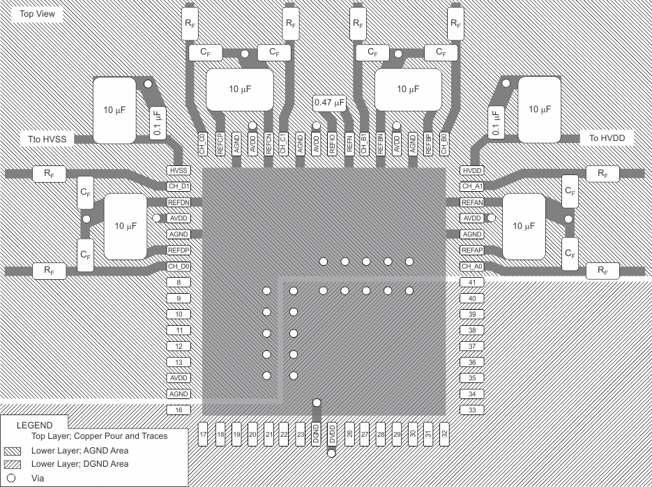
Depending on the circuit density on the board, placement of the analog and digital components, and the related current loops, a single solid ground plane for the entire printed circuit board (PCB) or dedicated analog and digital ground areas can be used. In case of separated ground areas, ensure that a low-impedance connection is between the analog and digital ground of the ADC by placing a bridge underneath (or next to) the ADC. Otherwise, even short undershoots on the digital interface with a value less than –300 mV lead to the conduction of ESD diodes, causing current to flow through the substrate and either degrading the analog performance or even damaging the device. Using a common ground plane underneath the device is recommended as a local ground reference for all xGND pins; see Figure 49. During PCB layout, care must be taken to avoid any return currents crossing sensitive analog areas or signals.
12.2 Layout Example
Figure 49 shows a layout recommendation for the ADS85x8 along with the proper decoupling and reference capacitors placement and connections. The layout recommendation takes into account the actual size of the components used.
