ZHCSGU6A september 2017 – july 2023 ADS8588H
PRODUCTION DATA
- 1
- 1 特性
- 2 应用
- 3 说明
- 4 Revision History
- 5 Pin Configuration and Functions
-
6 Specifications
- 6.1 Absolute Maximum Ratings
- 6.2 ESD Ratings
- 6.3 Recommended Operating Conditions
- 6.4 Thermal Information
- 6.5 Electrical Characteristics
- 6.6 Timing Requirements: CONVST Control
- 6.7 Timing Requirements: Data Read Operation
- 6.8 Timing Requirements: Parallel Data Read Operation, CS and RD Tied Together
- 6.9 Timing Requirements: Parallel Data Read Operation, CS and RD Separate
- 6.10 Timing Requirements: Serial Data Read Operation
- 6.11 Timing Requirements: Byte Mode Data Read Operation
- 6.12 Timing Requirements: Oversampling Mode
- 6.13 Timing Requirements: Exit Standby Mode
- 6.14 Timing Requirements: Exit Shutdown Mode
- 6.15 Switching Characteristics: CONVST Control
- 6.16 Switching Characteristics: Parallel Data Read Operation, CS and RD Tied Together
- 6.17 Switching Characteristics: Parallel Data Read Operation, CS and RD Separate
- 6.18 Switching Characteristics: Serial Data Read Operation
- 6.19 Switching Characteristics: Byte Mode Data Read Operation
- 6.20 Timing Diagrams
- 6.21 Typical Characteristics
-
7 Detailed Description
- 7.1 Overview
- 7.2 Functional Block Diagram
- 7.3 Feature Description
- 7.4
Device Functional Modes
- 7.4.1
Device Interface: Pin Description
- 7.4.1.1 REFSEL (Input)
- 7.4.1.2 RANGE (Input)
- 7.4.1.3 STBY (Input)
- 7.4.1.4 PAR/SER/BYTE SEL (Input)
- 7.4.1.5 CONVSTA, CONVSTB (Input)
- 7.4.1.6 RESET (Input)
- 7.4.1.7 RD/SCLK (Input)
- 7.4.1.8 CS (Input)
- 7.4.1.9 OS[2:0]
- 7.4.1.10 BUSY (Output)
- 7.4.1.11 FRSTDATA (Output)
- 7.4.1.12 DB15/BYTE SEL
- 7.4.1.13 DB14/HBEN
- 7.4.1.14 DB[13:9]
- 7.4.1.15 DB8/DOUTB
- 7.4.1.16 DB7/DOUTA
- 7.4.1.17 DB[6:0]
- 7.4.2 Device Modes of Operation
- 7.4.1
Device Interface: Pin Description
- 8 Application and Implementation
- 9 Device and Documentation Support
- 10Mechanical, Packaging, and Orderable Information
7.3.8.1 Internal Reference
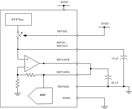
The device has an internal 2.5-V (nominal value) band-gap reference. In order to select the internal reference, the REFSEL pin must be tied high or connected to DVDD. When the internal reference is used, REFIN/REFOUT (pin 42) becomes an output pin with the internal reference value. A 10-µF (minimum) decoupling capacitor, as shown in Figure 7-6, is recommended to be placed between the REFIN/REFOUT pin and REFGND (pin 43). The capacitor must be placed as close to the REFIN/REFOUT pin as possible. The output impedance of the internal band gap creates a low-pass filter with this capacitor to band-limit the noise of the band-gap output. The use of a smaller capacitor increases the reference noise in the system, thus degrading SNR and SINAD performance. Do not use the REFIN/REFOUT pin to drive external ac or dc loads because of the limited current output capability of the pin. The REFIN/REFOUT pin can be used as a reference source if followed by a suitable op amp buffer.
 Figure 7-6 Device Connections for Using an Internal 2.5-V Reference
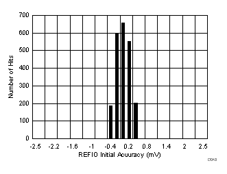
The device internal reference is factory trimmed to a maximum initial accuracy of ±2.5 mV. The histogram in Figure 7-7 shows the distribution of the internal voltage reference output.
 Figure 7-7 Internal Reference Accuracy at Room Temperature Histogram
The initial accuracy specification for the internal reference can be degraded if the die is exposed to any mechanical, thermal, or environmental stress (such as humidity). Heating the device when being soldered to a printed circuit board (PCB) and any subsequent solder reflow is a primary cause for shifts in the VREF value. The main cause of thermal hysteresis is a change in die stress and therefore is a function of the package, die-attach material, and molding compound, as well as the layout of the device.
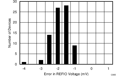
In order to illustrate this effect, 80 devices were soldered using lead-free solder paste with the suggested manufacturer reflow profile, as explained in the AN-2029 Handling & Process Recommendations application note. The internal voltage reference output is measured before and after the reflow process and Figure 7-8 shows the typical shift in value. Although all tested units exhibit a positive shift in the output voltages, negative shifts are also possible. The histogram in Figure 7-8 shows the typical shift for exposure to a single reflow profile. Exposure to multiple reflows, which is common on PCBs with surface-mount components on both sides, causes additional shifts in the output voltage. If the PCB is to be exposed to multiple reflows, solder the ADS8588H in the last pass to minimize device exposure to thermal stress.
 Figure 7-8 Solder Heat Shift Distribution Histogram
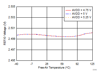
The internal reference is also temperature compensated to provide excellent temperature drift over an extended industrial temperature range of –40°C to +125°C. Figure 7-9 shows the variation of the internal reference voltage across temperature for different values of the AVDD supply voltage. The typical specified value of the reference voltage drift over temperature is 7.5 ppm/°C .
 Figure 7-9 Variation of Internal Reference Output (REFIN/REFOUT) vs Free-Air Temperature and Supply