ZHCSGU6A september 2017 – july 2023 ADS8588H
PRODUCTION DATA
- 1
- 1 特性
- 2 应用
- 3 说明
- 4 Revision History
- 5 Pin Configuration and Functions
-
6 Specifications
- 6.1 Absolute Maximum Ratings
- 6.2 ESD Ratings
- 6.3 Recommended Operating Conditions
- 6.4 Thermal Information
- 6.5 Electrical Characteristics
- 6.6 Timing Requirements: CONVST Control
- 6.7 Timing Requirements: Data Read Operation
- 6.8 Timing Requirements: Parallel Data Read Operation, CS and RD Tied Together
- 6.9 Timing Requirements: Parallel Data Read Operation, CS and RD Separate
- 6.10 Timing Requirements: Serial Data Read Operation
- 6.11 Timing Requirements: Byte Mode Data Read Operation
- 6.12 Timing Requirements: Oversampling Mode
- 6.13 Timing Requirements: Exit Standby Mode
- 6.14 Timing Requirements: Exit Shutdown Mode
- 6.15 Switching Characteristics: CONVST Control
- 6.16 Switching Characteristics: Parallel Data Read Operation, CS and RD Tied Together
- 6.17 Switching Characteristics: Parallel Data Read Operation, CS and RD Separate
- 6.18 Switching Characteristics: Serial Data Read Operation
- 6.19 Switching Characteristics: Byte Mode Data Read Operation
- 6.20 Timing Diagrams
- 6.21 Typical Characteristics
-
7 Detailed Description
- 7.1 Overview
- 7.2 Functional Block Diagram
- 7.3 Feature Description
- 7.4
Device Functional Modes
- 7.4.1
Device Interface: Pin Description
- 7.4.1.1 REFSEL (Input)
- 7.4.1.2 RANGE (Input)
- 7.4.1.3 STBY (Input)
- 7.4.1.4 PAR/SER/BYTE SEL (Input)
- 7.4.1.5 CONVSTA, CONVSTB (Input)
- 7.4.1.6 RESET (Input)
- 7.4.1.7 RD/SCLK (Input)
- 7.4.1.8 CS (Input)
- 7.4.1.9 OS[2:0]
- 7.4.1.10 BUSY (Output)
- 7.4.1.11 FRSTDATA (Output)
- 7.4.1.12 DB15/BYTE SEL
- 7.4.1.13 DB14/HBEN
- 7.4.1.14 DB[13:9]
- 7.4.1.15 DB8/DOUTB
- 7.4.1.16 DB7/DOUTA
- 7.4.1.17 DB[6:0]
- 7.4.2 Device Modes of Operation
- 7.4.1
Device Interface: Pin Description
- 8 Application and Implementation
- 9 Device and Documentation Support
- 10Mechanical, Packaging, and Orderable Information
7.3.8.2 External Reference
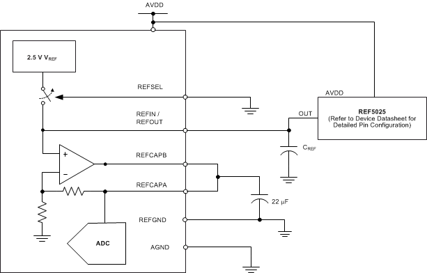
For applications that require a reference voltage with lower temperature drift or a common reference voltage for multiple devices, the ADS8588H offers a provision to use an external reference, using the internal buffer to drive the ADC reference pin. In order to select the external reference mode, either tie the REFSEL pin low or connect this pin to AGND. In this mode, an external 2.5-V reference must be applied at REFIN/REFOUT (pin 42), which becomes a high-impedance input pin. Any low-drift, small-size external reference can be used in this mode because the internal buffer is optimally designed to handle the dynamic loading on the ADC reference input. The output of the external reference must be filtered to minimize the resulting effect of the reference noise on system performance. Figure 7-10 shows a typical connection diagram for this mode.
 Figure 7-10 Device Connections for Using an External 2.5-V Reference
For closed-loop operation of the internal reference buffer, the REFCAPA and REFCAPB pins must be externally shorted together. The output of the internal reference buffer appears at the REFCAP pin. A minimum capacitance of 10 µF must be placed between the REFCAPA, REFCAPB pins and REFGND (pin 43). Do not use this internal reference buffer to drive external ac or dc loads because of the limited current output capability of the buffer.
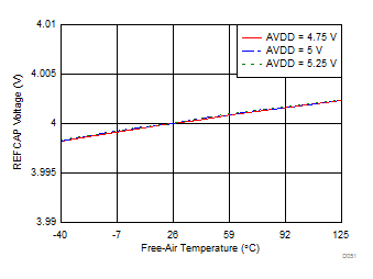
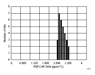
The performance of the internal buffer output (as shown in Figure 7-11) is very stable across the entire operating temperature range of –40°C to +125°C. The typical specified value of the reference buffer drift over temperature is 5 ppm/°C (Figure 7-12).


| Number of samples = 30 |