ZHCSGU5 September 2017 ADS8598H
PRODUCTION DATA.
- 1 特性
- 2 应用
- 3 说明
- 4 修订历史记录
- 5 Pin Configuration and Functions
-
6 Specifications
- 6.1 Absolute Maximum Ratings
- 6.2 ESD Ratings
- 6.3 Recommended Operating Conditions
- 6.4 Thermal Information
- 6.5 Electrical Characteristics
- 6.6 Timing Requirements: CONVST Control
- 6.7 Timing Requirements: Data Read Operation
- 6.8 Timing Requirements: Parallel Data Read Operation, CS and RD Tied Together
- 6.9 Timing Requirements: Parallel Data Read Operation, CS and RD Separate
- 6.10 Timing Requirements: Serial Data Read Operation
- 6.11 Timing Requirements: Byte Mode Data Read Operation
- 6.12 Timing Requirements: Oversampling Mode
- 6.13 Timing Requirements: Exit Standby Mode
- 6.14 Timing Requirements: Exit Shutdown Mode
- 6.15 Switching Characteristics: CONVST Control
- 6.16 Switching Characteristics: Parallel Data Read Operation, CS and RD Tied Together
- 6.17 Switching Characteristics: Parallel Data Read Operation, CS and RD Separate
- 6.18 Switching Characteristics: Serial Data Read Operation
- 6.19 Switching Characteristics: Byte Mode Data Read Operation
- 6.20 Typical Characteristics
-
7 Detailed Description
- 7.1 Overview
- 7.2 Functional Block Diagram
- 7.3 Feature Description
- 7.4
Device Functional Modes
- 7.4.1
Device Interface: Pin Description
- 7.4.1.1 REFSEL (Input)
- 7.4.1.2 RANGE (Input)
- 7.4.1.3 STBY (Input)
- 7.4.1.4 PAR/SER/BYTE SEL (Input)
- 7.4.1.5 CONVSTA, CONVSTB (Input)
- 7.4.1.6 RESET (Input)
- 7.4.1.7 RD/SCLK (Input)
- 7.4.1.8 CS (Input)
- 7.4.1.9 OS[2:0]
- 7.4.1.10 BUSY (Output)
- 7.4.1.11 FRSTDATA (Output)
- 7.4.1.12 DB15/BYTE SEL
- 7.4.1.13 DB14/HBEN
- 7.4.1.14 DB[13:9]
- 7.4.1.15 DB8/DOUTB
- 7.4.1.16 DB7/DOUTA
- 7.4.1.17 DB[6:0]
- 7.4.2 Device Modes of Operation
- 7.4.1
Device Interface: Pin Description
- 8 Application and Implementation
- 9 Power Supply Recommendations
- 10Layout
- 11器件和文档支持
- 12机械、封装和可订购信息
10 Layout
10.1 Layout Guidelines
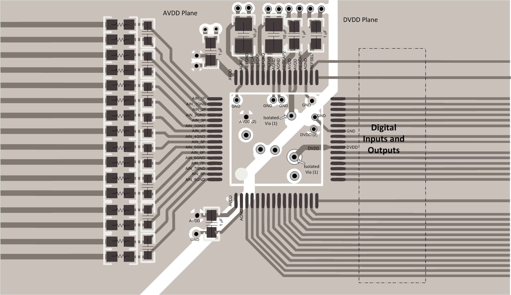
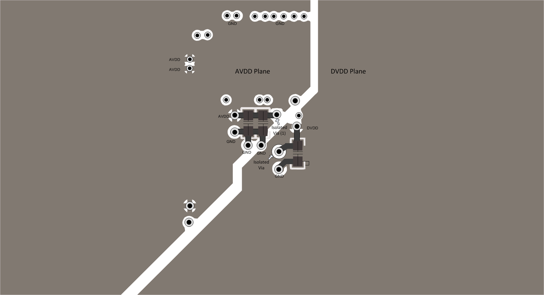
Figure 90 and Figure 91 illustrate a PCB layout example for the ADS8598H.
- Partition the PCB into analog and digital sections. Care must be taken to ensure that the analog signals are kept away from the digital lines. This layout helps keep the analog input and reference input signals away from the digital noise. In this layout example, the analog input and reference signals are routed on the left side of the board and the digital connections are routed on the right side of the board.
- Using a single common ground plane is strongly recommended. For designs requiring a split analog and digital ground planes, the analog and digital ground planes must be at the same potential joined together in close proximity to the devices.
- Power sources to the ADS8598H must be clean and well-bypassed. As a result of dynamic currents during conversion, each AVDD must have a decoupling capacitor to keep the supply voltage stable. Use wide traces or a dedicated analog supply plane to minimize trace inductance and reduce glitches. Using a 1-µF, X7R-grade, 0603-size ceramic capacitor is recommended in close proximity to each analog (AVDD) supply pin. Bypass capacitors for AVDD pins 1 and 48 are located on the top layer; see Figure 90. AVDD supply pins 37 and 38 are connected to bypass capacitors in the bottom layer using an isolated via (1); see Figure 91. A separate via (2) is used to connect the bypass capacitor to the AVDD plane.
- For decoupling the digital (DVDD) supply pin, a 1-µF, X7R-grade, 0603-size ceramic capacitor is recommended. The DVDD bypass capacitor is located in the bottom layer; see Figure 91.
- REFCAPA and REFCAPB must be shorted together and decoupled to REFGND using a 10-µF, X7R-grade, 0603-size ceramic capacitor placed in close proximity to the pins of the device. This capacitor is placed on the top layer and is directly connected to the device pins. Avoid placing vias between the REFCAPA, REFCAPB pins and the decoupling capacitor.
- The REFIN/REFOUT pin also must be decoupled to REFGND with a 10-µF, X7R-grade, 0603-size ceramic capacitor if the internal reference of the device is used. The capacitor must be placed on the top layer in close to the device pin. Avoid placing vias between the REFIN/REFOUT pin and the decoupling capacitor.
- The REGCAP1 and REGCAP2 pins must be decoupled to GND using a separate 1-µF, X7R-grade, 0603-size ceramic capacitor on each pin.
- All ground pins (AGND) must be connected to the ground plane using short, low-impedance paths and independent vias to the ground plane. Connect REFGND to the common GND plane.
- For the optional channel input low-pass filters, ceramic surface-mount capacitors, COG (NPO) ceramic capacitors provide the best capacitance precision. The type of dielectric used in COG (NPO) ceramic capacitors provides the most stable electrical properties over voltage, frequency, and temperature changes.

