ZHCSFU0B December 2016 – March 2021 ADS8661 , ADS8665
PRODUCTION DATA
- 1 特性
- 2 应用
- 3 说明
- 4 Revision History
- 5 Pin Configuration and Functions
-
6 Specifications
- 6.1 Absolute Maximum Ratings
- 6.2 ESD Ratings
- 6.3 Recommended Operating Conditions
- 6.4 Thermal Information
- 6.5 Electrical Characteristics
- 6.6 Timing Requirements: Conversion Cycle
- 6.7 Timing Requirements: Asynchronous Reset
- 6.8 Timing Requirements: SPI-Compatible Serial Interface
- 6.9 Timing Requirements: Source-Synchronous Serial Interface (External Clock)
- 6.10 Timing Requirements: Source-Synchronous Serial Interface (Internal Clock)
- 6.11 Timing Diagrams
- 6.12 Typical Characteristics
-
7 Detailed Description
- 7.1 Overview
- 7.2 Functional Block Diagram
- 7.3 Feature Description
- 7.4 Device Functional Modes
- 7.5 Programming
- 7.6
Register Maps
- 7.6.1
Device Configuration and Register Maps
- 7.6.1.1 DEVICE_ID_REG Register (address = 00h)
- 7.6.1.2 RST_PWRCTL_REG Register (address = 04h)
- 7.6.1.3 SDI_CTL_REG Register (address = 08h)
- 7.6.1.4 SDO_CTL_REG Register (address = 0Ch)
- 7.6.1.5 DATAOUT_CTL_REG Register (address = 10h)
- 7.6.1.6 RANGE_SEL_REG Register (address = 14h)
- 7.6.1.7 ALARM_REG Register (address = 20h)
- 7.6.1.8 ALARM_H_TH_REG Register (address = 24h)
- 7.6.1.9 ALARM_L_TH_REG Register (address = 28h)
- 7.6.1
Device Configuration and Register Maps
- 8 Application and Implementation
- 9 Power Supply Recommendations
- 10Layout
- 11Device and Documentation Support
7.3.7.2 External Reference
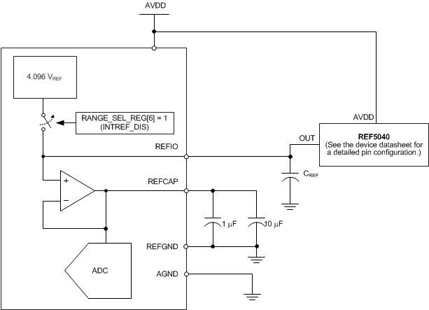
For applications that require a better reference voltage or a common reference voltage for multiple devices, the device provides a provision to use an external reference source along with an internal buffer to drive the ADC reference pin. In order to select the external reference mode, the INTREF_DIS bit of the RANGE_SEL_REG register must be programmed to logic 1. In this mode, an external 4.096-V reference must be applied at the REFIO pin, which functions as an input. Any low-power, low-drift, or small-size external reference can be used in this mode because the internal buffer is optimally designed to handle the dynamic loading on the REFCAP pin that is internally connected to the ADC reference input. The output of the external reference must be appropriately filtered to minimize the resulting effect of the reference noise on system performance. A typical connection diagram for this mode is shown in Figure 7-12.
 Figure 7-12 Device Connections for Using an External 4.096-V Reference
The output of the internal reference buffer appears at the REFCAP pin. A minimum capacitance of 10 µF must be placed between the REFCAP and REFGND pins. Place another capacitor of 1 µF as close to the REFCAP pin as possible for decoupling high-frequency signals. Do not use the internal buffer to drive external ac or dc loads because of the limited current output capability of this buffer.
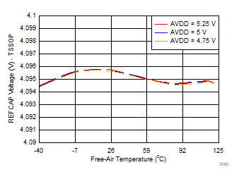
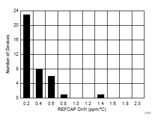
The performance of the internal buffer output is very stable across the entire operating temperature range of –40°C to +125°C. Figure 7-13 shows the variation in the REFCAP output across temperature for different values of the AVDD supply voltage. The typical specified value of the reference buffer drift over temperature is 0.5 ppm/°C, as shown in Figure 7-14, and the maximum specified temperature drift is equal to 2 ppm/°C.


| AVDD = 5 V, number of devices = 30, ΔT = –40°C to +125°C |