ZHCSFT9B December 2016 – March 2021 ADS8671 , ADS8675
PRODUCTION DATA
- 1 特性
- 2 应用
- 3 说明
- 4 Revision History
- 5 Pin Configuration and Functions
-
6 Specifications
- 6.1 Absolute Maximum Ratings
- 6.2 ESD Ratings
- 6.3 Recommended Operating Conditions
- 6.4 Thermal Information
- 6.5 Electrical Characteristics
- 6.6 Timing Requirements: Conversion Cycle
- 6.7 Timing Requirements: Asynchronous Reset
- 6.8 Timing Requirements: SPI-Compatible Serial Interface
- 6.9 Timing Requirements: Source-Synchronous Serial Interface (External Clock)
- 6.10 Timing Requirements: Source-Synchronous Serial Interface (Internal Clock)
- 6.11 Timing Diagrams
- 6.12 Typical Characteristics
-
7 Detailed Description
- 7.1 Overview
- 7.2 Functional Block Diagram
- 7.3 Feature Description
- 7.4 Device Functional Modes
- 7.5 Programming
- 7.6
Register Maps
- 7.6.1
Device Configuration and Register Maps
- 7.6.1.1 DEVICE_ID_REG Register (address = 00h)
- 7.6.1.2 RST_PWRCTL_REG Register (address = 04h)
- 7.6.1.3 SDI_CTL_REG Register (address = 08h)
- 7.6.1.4 SDO_CTL_REG Register (address = 0Ch)
- 7.6.1.5 DATAOUT_CTL_REG Register (address = 10h)
- 7.6.1.6 RANGE_SEL_REG Register (address = 14h)
- 7.6.1.7 ALARM_REG Register (address = 20h)
- 7.6.1.8 ALARM_H_TH_REG Register (address = 24h)
- 7.6.1.9 ALARM_L_TH_REG Register (address = 28h)
- 7.6.1
Device Configuration and Register Maps
- 8 Application and Implementation
- 9 Power Supply Recommendations
- 10Layout
- 11Device and Documentation Support
6.11 Timing Diagrams
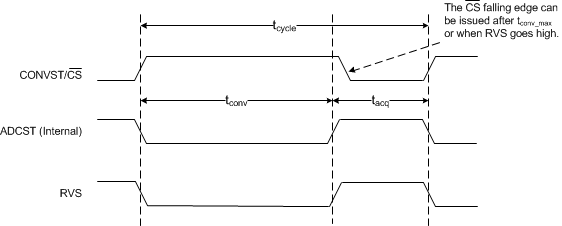 Figure 6-1 Conversion Cycle Timing Diagram
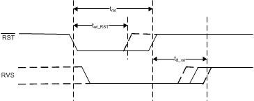 Figure 6-2 Asynchronous Reset Timing Diagram
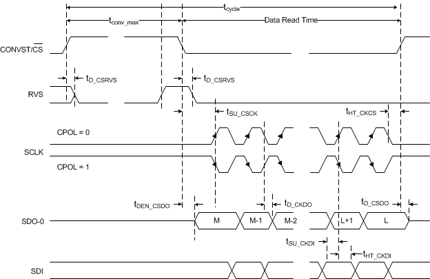 Figure 6-3 Standard
SPI Interface Timing Diagram for CPHA = 0
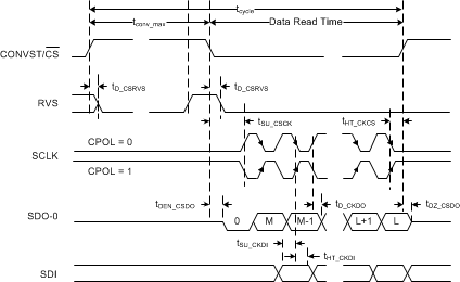 Figure 6-4 Standard
SPI Interface Timing Diagram for CPHA = 1
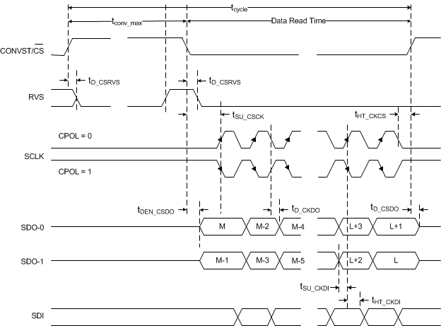 Figure 6-5 multiSPI
Interface Timing Diagram for Dual SDO-x and CPHA = 0
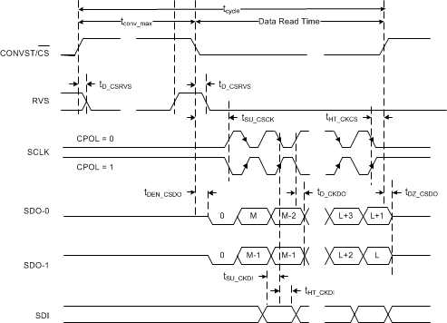 Figure 6-6 multiSPI
Interface Timing Diagram for Dual SDO-x and CPHA = 1
 Figure 6-7 multiSPI
Source-Synchronous External Clock Serial Interface Timing Diagram
 Figure 6-8 multiSPI
Source-Synchronous Internal Clock Serial Interface Timing Diagram