ZHCSEV3E
February 2016 – August 2022
ADS8681
,
ADS8685
,
ADS8689
PRODUCTION DATA
1
特性
2
应用
3
说明
4
Revision History
5
Pin Configuration and Functions
6
Specifications
6.1
Absolute Maximum Ratings
6.2
ESD Ratings
6.3
Recommended Operating Conditions
6.4
Thermal Information
6.5
Electrical Characteristics
6.6
Timing Requirements: Conversion Cycle
6.7
Timing Requirements: Asynchronous Reset
6.8
Timing Requirements: SPI-Compatible Serial Interface
6.9
Timing Requirements: Source-Synchronous Serial Interface (External Clock)
6.10
Timing Requirements: Source-Synchronous Serial Interface (Internal Clock)
6.11
Timing Diagrams
6.12
Typical Characteristics
7
Detailed Description
7.1
Overview
7.2
Functional Block Diagram
7.3
Feature Description
7.3.1
Analog Input Structure
7.3.2
Analog Input Impedance
7.3.3
Input Protection Circuit
7.3.4
Programmable Gain Amplifier (PGA)
7.3.5
Second-Order, Low-Pass Filter (LPF)
7.3.6
ADC Driver
7.3.7
Reference
7.3.7.1
Internal Reference
7.3.7.2
External Reference
7.3.8
ADC Transfer Function
7.3.9
Alarm Features
7.3.9.1
Input Alarm
7.3.9.2
AVDD Alarm
7.4
Device Functional Modes
7.4.1
Host-to-Device Connection Topologies
7.4.1.1
Single Device: All multiSPI Options
7.4.1.2
Single Device: Standard SPI Interface
7.4.1.3
Multiple Devices: Daisy-Chain Topology
7.4.2
Device Operational Modes
7.4.2.1
RESET State
7.4.2.2
ACQ State
7.4.2.3
CONV State
7.5
Programming
7.5.1
Data Transfer Frame
7.5.2
Input Command Word and Register Write Operation
7.5.3
Output Data Word
7.5.4
Data Transfer Protocols
7.5.4.1
Protocols for Configuring the Device
7.5.4.2
Protocols for Reading From the Device
7.5.4.2.1
Legacy, SPI-Compatible (SYS-xy-S) Protocols with a Single SDO-x
7.5.4.2.2
Legacy, SPI-Compatible (SYS-xy-S) Protocols With Dual SDO-x
7.5.4.2.3
Source-Synchronous (SRC) Protocols
7.5.4.2.3.1
Output Clock Source Options
7.5.4.2.3.2
Output Bus Width Options
7.6
Register Maps
7.6.1
Device Configuration and Register Maps
7.6.1.1
DEVICE_ID_REG Register (address = 00h)
7.6.1.2
RST_PWRCTL_REG Register (address = 04h)
7.6.1.3
SDI_CTL_REG Register (address = 08h)
7.6.1.4
SDO_CTL_REG Register (address = 0Ch)
7.6.1.5
DATAOUT_CTL_REG Register (address = 10h)
7.6.1.6
RANGE_SEL_REG Register (address = 14h)
7.6.1.7
ALARM_REG Register (address = 20h)
7.6.1.8
ALARM_H_TH_REG Register (address = 24h)
7.6.1.9
ALARM_L_TH_REG Register (address = 28h)
8
Application and Implementation
8.1
Application Information
8.2
Typical Application
8.2.1
Design Requirements
8.2.2
Detailed Design Procedure
8.2.3
Application Curves
8.3
Power Supply Recommendations
8.3.1
Power Supply Decoupling
8.3.2
Power Saving
8.3.2.1
NAP Mode
8.3.2.2
Power-Down (PD) Mode
8.4
Layout
8.4.1
Layout Guidelines
8.4.2
Layout Example
9
Device and Documentation Support
9.1
Documentation Support
9.1.1
Related Documentation
9.2
接收文档更新通知
9.3
支持资源
9.4
Trademarks
9.5
Electrostatic Discharge Caution
9.6
术语表
10
Mechanical, Packaging, and Orderable Information
封装选项
机械数据 (封装 | 引脚)
RUM|16
MPQF223A
PW|16
MPDS361A
散热焊盘机械数据 (封装 | 引脚)
RUM|16
QFND157C
订购信息
zhcsev3e_oa
zhcsev3e_pm
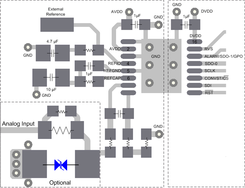
8.4.2
Layout Example
Figure 8-12
Board Layout for the
ADS868x
千亿体育app官网登录(中国)官方网站IOS/安卓通用版/手机APP
|
米乐app下载官网(中国)|ios|Android/通用版APP最新版
|
米乐|米乐·M6(中国大陆)官方网站
|
千亿体育登陆地址
|
华体会体育(中国)HTH·官方网站
|
千赢qy国际_全站最新版千赢qy国际V6.2.14安卓/IOS下载
|
18新利网v1.2.5|中国官方网站
|
bob电竞真人(中国官网)安卓/ios苹果/电脑版【1.97.95版下载】
|
千亿体育app官方下载(中国)官方网站IOS/安卓/手机APP下载安装
|