ZHCSEV3E February 2016 – August 2022 ADS8681 , ADS8685 , ADS8689
PRODUCTION DATA
- 1 特性
- 2 应用
- 3 说明
- 4 Revision History
- 5 Pin Configuration and Functions
-
6 Specifications
- 6.1 Absolute Maximum Ratings
- 6.2 ESD Ratings
- 6.3 Recommended Operating Conditions
- 6.4 Thermal Information
- 6.5 Electrical Characteristics
- 6.6 Timing Requirements: Conversion Cycle
- 6.7 Timing Requirements: Asynchronous Reset
- 6.8 Timing Requirements: SPI-Compatible Serial Interface
- 6.9 Timing Requirements: Source-Synchronous Serial Interface (External Clock)
- 6.10 Timing Requirements: Source-Synchronous Serial Interface (Internal Clock)
- 6.11 Timing Diagrams
- 6.12 Typical Characteristics
-
7 Detailed Description
- 7.1 Overview
- 7.2 Functional Block Diagram
- 7.3 Feature Description
- 7.4 Device Functional Modes
- 7.5 Programming
- 7.6
Register Maps
- 7.6.1
Device Configuration and Register Maps
- 7.6.1.1 DEVICE_ID_REG Register (address = 00h)
- 7.6.1.2 RST_PWRCTL_REG Register (address = 04h)
- 7.6.1.3 SDI_CTL_REG Register (address = 08h)
- 7.6.1.4 SDO_CTL_REG Register (address = 0Ch)
- 7.6.1.5 DATAOUT_CTL_REG Register (address = 10h)
- 7.6.1.6 RANGE_SEL_REG Register (address = 14h)
- 7.6.1.7 ALARM_REG Register (address = 20h)
- 7.6.1.8 ALARM_H_TH_REG Register (address = 24h)
- 7.6.1.9 ALARM_L_TH_REG Register (address = 28h)
- 7.6.1
Device Configuration and Register Maps
- 8 Application and Implementation
- 9 Device and Documentation Support
- 10Mechanical, Packaging, and Orderable Information
封装选项
机械数据 (封装 | 引脚)
散热焊盘机械数据 (封装 | 引脚)
- RUM|16
订购信息
7.3.8 ADC Transfer Function
The device supports a pseudo-differential input supporting both bipolar and unipolar input ranges. The output of the device is in straight-binary format for both bipolar and unipolar input ranges.
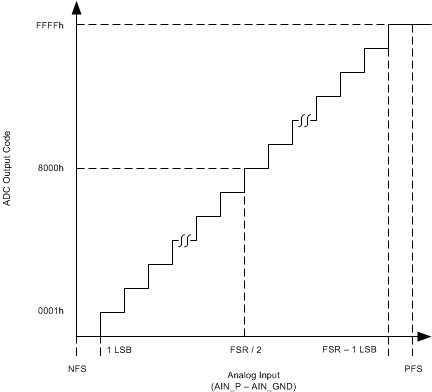
The ideal transfer characteristic for all input ranges is shown in Figure 7-19. The full-scale range (FSR) for each input signal is equal to the difference between the positive full-scale (PFS) input voltage and the negative full-scale (NFS) input voltage. The LSB size is equal to FSR / 216. For a reference voltage of VREF = 4.096 V, the LSB values corresponding to the different input ranges are listed in Table 7-4.
 Figure 7-19 Device Transfer Function (Straight-Binary Format)
Table 7-4 ADC LSB Values for Different Input Ranges (VREF = 4.096 V)
| INPUT RANGE | POSITIVE FULL-SCALE (V) | NEGATIVE FULL-SCALE (V) | FULL-SCALE RANGE (V) |
LSB |
|---|---|---|---|---|
| ±3 × VREF | 12.288 | –12.288 | 24.576 | 375.0 µV |
| ±2.5 × VREF | 10.24 | –10.24 | 20.48 | 312.5 µV |
| ±1.5 × VREF | 6.144 | –6.144 | 12.288 | 187.5 µV |
| ±1.25 × VREF | 5.12 | –5.12 | 10.24 | 156.25 µV |
| ±0.625 × VREF | 2.56 | –2.56 | 5.12 | 78.125 µV |
| 0 to 3 × VREF | 12.288 | 0 | 12.288 | 187.5 µV |
| 0 to 2.5 × VREF | 10.24 | 0 | 10.24 | 156.25 µV |
| 0 to 1.5 × VREF | 6.144 | 0 | 6.144 | 93.75 µV |
| 0 to 1.25 × VREF | 5.12 | 0 | 5.12 | 78.125 µV |