ZHCSEV3E February 2016 – August 2022 ADS8681 , ADS8685 , ADS8689
PRODUCTION DATA
- 1 特性
- 2 应用
- 3 说明
- 4 Revision History
- 5 Pin Configuration and Functions
-
6 Specifications
- 6.1 Absolute Maximum Ratings
- 6.2 ESD Ratings
- 6.3 Recommended Operating Conditions
- 6.4 Thermal Information
- 6.5 Electrical Characteristics
- 6.6 Timing Requirements: Conversion Cycle
- 6.7 Timing Requirements: Asynchronous Reset
- 6.8 Timing Requirements: SPI-Compatible Serial Interface
- 6.9 Timing Requirements: Source-Synchronous Serial Interface (External Clock)
- 6.10 Timing Requirements: Source-Synchronous Serial Interface (Internal Clock)
- 6.11 Timing Diagrams
- 6.12 Typical Characteristics
-
7 Detailed Description
- 7.1 Overview
- 7.2 Functional Block Diagram
- 7.3 Feature Description
- 7.4 Device Functional Modes
- 7.5 Programming
- 7.6
Register Maps
- 7.6.1
Device Configuration and Register Maps
- 7.6.1.1 DEVICE_ID_REG Register (address = 00h)
- 7.6.1.2 RST_PWRCTL_REG Register (address = 04h)
- 7.6.1.3 SDI_CTL_REG Register (address = 08h)
- 7.6.1.4 SDO_CTL_REG Register (address = 0Ch)
- 7.6.1.5 DATAOUT_CTL_REG Register (address = 10h)
- 7.6.1.6 RANGE_SEL_REG Register (address = 14h)
- 7.6.1.7 ALARM_REG Register (address = 20h)
- 7.6.1.8 ALARM_H_TH_REG Register (address = 24h)
- 7.6.1.9 ALARM_L_TH_REG Register (address = 28h)
- 7.6.1
Device Configuration and Register Maps
- 8 Application and Implementation
- 9 Device and Documentation Support
- 10Mechanical, Packaging, and Orderable Information
封装选项
机械数据 (封装 | 引脚)
散热焊盘机械数据 (封装 | 引脚)
- RUM|16
订购信息
7.5.4.2.1 Legacy, SPI-Compatible (SYS-xy-S) Protocols with a Single SDO-x
As shown in Table 7-9, the host controller can use any of the four legacy, SPI-compatible protocols (SPI-00-S, SPI-01-S, SPI-10-S, or SPI-11-S) to read data from the device.
| PROTOCOL | SCLK POLARITY (At CS Falling Edge) |
SCLK PHASE (Capture Edge) |
MSB BIT LAUNCH EDGE | SDI_CTL_REG | SDO_CTL_REG | DIAGRAM |
|---|---|---|---|---|---|---|
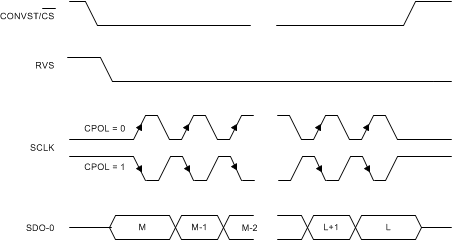
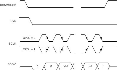
| SPI-00-S | Low | Rising | CS falling | 00h | 00h | Figure 7-32 |
| SPI-01-S | Low | Falling | 1st SCLK rising | 01h | 00h | Figure 7-32 |
| SPI-10-S | High | Falling | CS falling | 02h | 00h | Figure 7-33 |
| SPI-11-S | High | Rising | 1st SCLK falling | 03h | 00h | Figure 7-33 |
On power-up or after coming out of any asynchronous reset, the device supports the SPI-00-S protocol for data read and data write operations. To select a different SPI-compatible protocol for both the data transfer operations:
- Program the SDI_MODE[1:0] bits in the SDI_CTL_REG register. This first write operation must adhere to the SPI-00-S protocol. Any subsequent data transfer frames must adhere to the newly-selected protocol.
- Set the SDO_MODE[1:0] bits = 00b in the SDO_CTL_REG register.
The SPI transfer protocol selected by configuring the SDI_MODE[1:0] bits in the SDI_CTL_REG register determines the data transfer protocol for both write and read operations. Either data can be read from the device using the selected SPI protocol by configuring the SDO_MODE[1:0] bits = 00b in the SDO_CTL_REG register, or one of the SRC protocols can be selected for data read, as explained in the Section 7.5.4.2.3 section.
When using any of the SPI-compatible protocols, the RVS output remains low throughout the data transfer frame; see the Section 6.8 table for associated timing parameters.
Figure 7-32 and Figure 7-33 explain the details of the four protocols. As explained in the Section 7.5.1 section, the host controller can use a short data transfer frame to read only the required number of MSB bits from the 32-bit output data word.
If the host controller uses a long data transfer frame with SDO_CNTL_REG[7:0] = 00h, then the device exhibits daisy-chain operation (see the Section 7.4.1.3 section).
 Figure 7-32 Standard SPI Timing Protocol
(CPHA = 0, Single SDO-x)
 Figure 7-33 Standard SPI Timing Protocol
(CPHA = 1, Single SDO-x)