ZHCSEV3E February   2016  – August 2022 ADS8681 , ADS8685 , ADS8689

PRODUCTION DATA  

  1. 特性
  2. 应用
  3. 说明
  4. Revision History
  5. Pin Configuration and Functions
  6. Specifications
    1. 6.1  Absolute Maximum Ratings
    2. 6.2  ESD Ratings
    3. 6.3  Recommended Operating Conditions
    4. 6.4  Thermal Information
    5. 6.5  Electrical Characteristics
    6. 6.6  Timing Requirements: Conversion Cycle
    7. 6.7  Timing Requirements: Asynchronous Reset
    8. 6.8  Timing Requirements: SPI-Compatible Serial Interface
    9. 6.9  Timing Requirements: Source-Synchronous Serial Interface (External Clock)
    10. 6.10 Timing Requirements: Source-Synchronous Serial Interface (Internal Clock)
    11. 6.11 Timing Diagrams
    12. 6.12 Typical Characteristics
  7. Detailed Description
    1. 7.1 Overview
    2. 7.2 Functional Block Diagram
    3. 7.3 Feature Description
      1. 7.3.1 Analog Input Structure
      2. 7.3.2 Analog Input Impedance
      3. 7.3.3 Input Protection Circuit
      4. 7.3.4 Programmable Gain Amplifier (PGA)
      5. 7.3.5 Second-Order, Low-Pass Filter (LPF)
      6. 7.3.6 ADC Driver
      7. 7.3.7 Reference
        1. 7.3.7.1 Internal Reference
        2. 7.3.7.2 External Reference
      8. 7.3.8 ADC Transfer Function
      9. 7.3.9 Alarm Features
        1. 7.3.9.1 Input Alarm
        2. 7.3.9.2 AVDD Alarm
    4. 7.4 Device Functional Modes
      1. 7.4.1 Host-to-Device Connection Topologies
        1. 7.4.1.1 Single Device: All multiSPI Options
        2. 7.4.1.2 Single Device: Standard SPI Interface
        3. 7.4.1.3 Multiple Devices: Daisy-Chain Topology
      2. 7.4.2 Device Operational Modes
        1. 7.4.2.1 RESET State
        2. 7.4.2.2 ACQ State
        3. 7.4.2.3 CONV State
    5. 7.5 Programming
      1. 7.5.1 Data Transfer Frame
      2. 7.5.2 Input Command Word and Register Write Operation
      3. 7.5.3 Output Data Word
      4. 7.5.4 Data Transfer Protocols
        1. 7.5.4.1 Protocols for Configuring the Device
        2. 7.5.4.2 Protocols for Reading From the Device
          1. 7.5.4.2.1 Legacy, SPI-Compatible (SYS-xy-S) Protocols with a Single SDO-x
          2. 7.5.4.2.2 Legacy, SPI-Compatible (SYS-xy-S) Protocols With Dual SDO-x
          3. 7.5.4.2.3 Source-Synchronous (SRC) Protocols
            1. 7.5.4.2.3.1 Output Clock Source Options
            2. 7.5.4.2.3.2 Output Bus Width Options
    6. 7.6 Register Maps
      1. 7.6.1 Device Configuration and Register Maps
        1. 7.6.1.1 DEVICE_ID_REG Register (address = 00h)
        2. 7.6.1.2 RST_PWRCTL_REG Register (address = 04h)
        3. 7.6.1.3 SDI_CTL_REG Register (address = 08h)
        4. 7.6.1.4 SDO_CTL_REG Register (address = 0Ch)
        5. 7.6.1.5 DATAOUT_CTL_REG Register (address = 10h)
        6. 7.6.1.6 RANGE_SEL_REG Register (address = 14h)
        7. 7.6.1.7 ALARM_REG Register (address = 20h)
        8. 7.6.1.8 ALARM_H_TH_REG Register (address = 24h)
        9. 7.6.1.9 ALARM_L_TH_REG Register (address = 28h)
  8. Application and Implementation
    1. 8.1 Application Information
    2. 8.2 Typical Application
      1. 8.2.1 Design Requirements
      2. 8.2.2 Detailed Design Procedure
      3. 8.2.3 Application Curves
    3. 8.3 Power Supply Recommendations
      1. 8.3.1 Power Supply Decoupling
      2. 8.3.2 Power Saving
        1. 8.3.2.1 NAP Mode
        2. 8.3.2.2 Power-Down (PD) Mode
    4. 8.4 Layout
      1. 8.4.1 Layout Guidelines
      2. 8.4.2 Layout Example
  9. Device and Documentation Support
    1. 9.1 Documentation Support
      1. 9.1.1 Related Documentation
    2. 9.2 接收文档更新通知
    3. 9.3 支持资源
    4. 9.4 Trademarks
    5. 9.5 Electrostatic Discharge Caution
    6. 9.6 术语表
  10. 10Mechanical, Packaging, and Orderable Information

封装选项

机械数据 (封装 | 引脚)
散热焊盘机械数据 (封装 | 引脚)
订购信息

Power Supply Decoupling

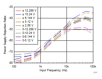
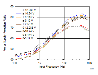
The AVDD supply pins must be decoupled with AGND by using a minimum 10-µF and 1-µF capacitor on each supply. Place the 1-µF capacitor as close to the supply pins as possible. Place a minimum 10-µF decoupling capacitor very close to the DVDD supply to provide the high-frequency digital switching current. The effect of using the decoupling capacitor is illustrated in the difference between the power-supply rejection ratio (PSRR) performance of the device. Figure 8-10 shows the PSRR of the device without using a decoupling capacitor. The PSRR improves when the decoupling capacitors are used, as shown in Figure 8-11.
GUID-AD8D8D8A-6A3A-49E8-9BD7-017AC4E8A861-low.gif
Figure 8-10 PSRR Without a Decoupling Capacitor
GUID-E7DB0215-86DE-430C-930F-71AB55C1213E-low.gif
Figure 8-11 PSRR With a Decoupling Capacitor