ZHCSFT8B December   2016  – March 2021 ADS8691 , ADS8695 , ADS8699

PRODUCTION DATA  

  1. 特性
  2. 应用
  3. 说明
  4. Revision History
  5. Pin Configuration and Functions
  6. Specifications
    1. 6.1  Absolute Maximum Ratings
    2. 6.2  ESD Ratings
    3. 6.3  Recommended Operating Conditions
    4. 6.4  Thermal Information
    5. 6.5  Electrical Characteristics
    6. 6.6  Timing Requirements: Conversion Cycle
    7. 6.7  Timing Requirements: Asynchronous Reset
    8. 6.8  Timing Requirements: SPI-Compatible Serial Interface
    9. 6.9  Timing Requirements: Source-Synchronous Serial Interface (External Clock)
    10. 6.10 Timing Requirements: Source-Synchronous Serial Interface (Internal Clock)
    11. 6.11 Timing Diagrams
    12. 6.12 Typical Characteristics
  7. Detailed Description
    1. 7.1 Overview
    2. 7.2 Functional Block Diagram
    3. 7.3 Feature Description
      1. 7.3.1 Analog Input Structure
      2. 7.3.2 Analog Input Impedance
      3. 7.3.3 Input Protection Circuit
      4. 7.3.4 Programmable Gain Amplifier (PGA)
      5. 7.3.5 Second-Order, Low-Pass Filter (LPF)
      6. 7.3.6 ADC Driver
      7. 7.3.7 Reference
        1. 7.3.7.1 Internal Reference
        2. 7.3.7.2 External Reference
      8. 7.3.8 ADC Transfer Function
      9. 7.3.9 Alarm Features
        1. 7.3.9.1 Input Alarm
        2. 7.3.9.2 AVDD Alarm
    4. 7.4 Device Functional Modes
      1. 7.4.1 Host-to-Device Connection Topologies
        1. 7.4.1.1 Single Device: All multiSPI Options
        2. 7.4.1.2 Single Device: Standard SPI Interface
        3. 7.4.1.3 Multiple Devices: Daisy-Chain Topology
      2. 7.4.2 Device Operational Modes
        1. 7.4.2.1 RESET State
        2. 7.4.2.2 ACQ State
        3. 7.4.2.3 CONV State
    5. 7.5 Programming
      1. 7.5.1 Data Transfer Frame
      2. 7.5.2 Input Command Word and Register Write Operation
      3. 7.5.3 Output Data Word
      4. 7.5.4 Data Transfer Protocols
        1. 7.5.4.1 Protocols for Configuring the Device
        2. 7.5.4.2 Protocols for Reading From the Device
          1. 7.5.4.2.1 Legacy, SPI-Compatible (SYS-xy-S) Protocols with a Single SDO-x
          2. 7.5.4.2.2 Legacy, SPI-Compatible (SYS-xy-S) Protocols With Dual SDO-x
          3. 7.5.4.2.3 Source-Synchronous (SRC) Protocols
            1. 7.5.4.2.3.1 Output Clock Source Options
            2. 7.5.4.2.3.2 Output Bus Width Options
    6. 7.6 Register Maps
      1. 7.6.1 Device Configuration and Register Maps
        1. 7.6.1.1 DEVICE_ID_REG Register (address = 00h)
        2. 7.6.1.2 RST_PWRCTL_REG Register (address = 04h)
        3. 7.6.1.3 SDI_CTL_REG Register (address = 08h)
        4. 7.6.1.4 SDO_CTL_REG Register (address = 0Ch)
        5. 7.6.1.5 DATAOUT_CTL_REG Register (address = 10h)
        6. 7.6.1.6 RANGE_SEL_REG Register (address = 14h)
        7. 7.6.1.7 ALARM_REG Register (address = 20h)
        8. 7.6.1.8 ALARM_H_TH_REG Register (address = 24h)
        9. 7.6.1.9 ALARM_L_TH_REG Register (address = 28h)
  8. Application and Implementation
    1. 8.1 Application Information
    2. 8.2 Typical Application
      1. 8.2.1 Design Requirements
      2. 8.2.2 Detailed Design Procedure
      3. 8.2.3 Application Curves
  9. Power Supply Recommendations
    1. 9.1 Power Supply Decoupling
    2. 9.2 Power Saving
      1. 9.2.1 NAP Mode
      2. 9.2.2 Power-Down (PD) Mode
  10. 10Layout
    1. 10.1 Layout Guidelines
    2. 10.2 Layout Example
  11. 11Device and Documentation Support
    1. 11.1 Documentation Support
      1. 11.1.1 Related Documentation
    2. 11.2 接收文档更新通知
    3. 11.3 支持资源
    4. 11.4 Trademarks
    5. 11.5 静电放电警告
    6. 11.6 术语表

封装选项

机械数据 (封装 | 引脚)
散热焊盘机械数据 (封装 | 引脚)
订购信息

Single Device: Standard SPI Interface

Figure 7-21 shows the minimum pin interface for applications using a standard SPI protocol.
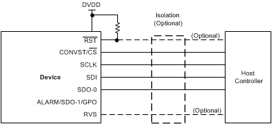
GUID-95231AB2-4066-4EA7-8C98-8D61388C7542-low.gifFigure 7-21 Standard SPI Protocol Pin Configuration

The CONVST/CS, SCLK, SDI, and SDO-0 pins constitute a standard SPI port of the host controller. The RST pin can be tied to DVDD. The RVS pin can be monitored for timing benefits. The ALARM/SDO-1/GPO pin may not have any external connection.