ZHCSFT8B December   2016  – March 2021 ADS8691 , ADS8695 , ADS8699

PRODUCTION DATA  

  1. 特性
  2. 应用
  3. 说明
  4. Revision History
  5. Pin Configuration and Functions
  6. Specifications
    1. 6.1  Absolute Maximum Ratings
    2. 6.2  ESD Ratings
    3. 6.3  Recommended Operating Conditions
    4. 6.4  Thermal Information
    5. 6.5  Electrical Characteristics
    6. 6.6  Timing Requirements: Conversion Cycle
    7. 6.7  Timing Requirements: Asynchronous Reset
    8. 6.8  Timing Requirements: SPI-Compatible Serial Interface
    9. 6.9  Timing Requirements: Source-Synchronous Serial Interface (External Clock)
    10. 6.10 Timing Requirements: Source-Synchronous Serial Interface (Internal Clock)
    11. 6.11 Timing Diagrams
    12. 6.12 Typical Characteristics
  7. Detailed Description
    1. 7.1 Overview
    2. 7.2 Functional Block Diagram
    3. 7.3 Feature Description
      1. 7.3.1 Analog Input Structure
      2. 7.3.2 Analog Input Impedance
      3. 7.3.3 Input Protection Circuit
      4. 7.3.4 Programmable Gain Amplifier (PGA)
      5. 7.3.5 Second-Order, Low-Pass Filter (LPF)
      6. 7.3.6 ADC Driver
      7. 7.3.7 Reference
        1. 7.3.7.1 Internal Reference
        2. 7.3.7.2 External Reference
      8. 7.3.8 ADC Transfer Function
      9. 7.3.9 Alarm Features
        1. 7.3.9.1 Input Alarm
        2. 7.3.9.2 AVDD Alarm
    4. 7.4 Device Functional Modes
      1. 7.4.1 Host-to-Device Connection Topologies
        1. 7.4.1.1 Single Device: All multiSPI Options
        2. 7.4.1.2 Single Device: Standard SPI Interface
        3. 7.4.1.3 Multiple Devices: Daisy-Chain Topology
      2. 7.4.2 Device Operational Modes
        1. 7.4.2.1 RESET State
        2. 7.4.2.2 ACQ State
        3. 7.4.2.3 CONV State
    5. 7.5 Programming
      1. 7.5.1 Data Transfer Frame
      2. 7.5.2 Input Command Word and Register Write Operation
      3. 7.5.3 Output Data Word
      4. 7.5.4 Data Transfer Protocols
        1. 7.5.4.1 Protocols for Configuring the Device
        2. 7.5.4.2 Protocols for Reading From the Device
          1. 7.5.4.2.1 Legacy, SPI-Compatible (SYS-xy-S) Protocols with a Single SDO-x
          2. 7.5.4.2.2 Legacy, SPI-Compatible (SYS-xy-S) Protocols With Dual SDO-x
          3. 7.5.4.2.3 Source-Synchronous (SRC) Protocols
            1. 7.5.4.2.3.1 Output Clock Source Options
            2. 7.5.4.2.3.2 Output Bus Width Options
    6. 7.6 Register Maps
      1. 7.6.1 Device Configuration and Register Maps
        1. 7.6.1.1 DEVICE_ID_REG Register (address = 00h)
        2. 7.6.1.2 RST_PWRCTL_REG Register (address = 04h)
        3. 7.6.1.3 SDI_CTL_REG Register (address = 08h)
        4. 7.6.1.4 SDO_CTL_REG Register (address = 0Ch)
        5. 7.6.1.5 DATAOUT_CTL_REG Register (address = 10h)
        6. 7.6.1.6 RANGE_SEL_REG Register (address = 14h)
        7. 7.6.1.7 ALARM_REG Register (address = 20h)
        8. 7.6.1.8 ALARM_H_TH_REG Register (address = 24h)
        9. 7.6.1.9 ALARM_L_TH_REG Register (address = 28h)
  8. Application and Implementation
    1. 8.1 Application Information
    2. 8.2 Typical Application
      1. 8.2.1 Design Requirements
      2. 8.2.2 Detailed Design Procedure
      3. 8.2.3 Application Curves
  9. Power Supply Recommendations
    1. 9.1 Power Supply Decoupling
    2. 9.2 Power Saving
      1. 9.2.1 NAP Mode
      2. 9.2.2 Power-Down (PD) Mode
  10. 10Layout
    1. 10.1 Layout Guidelines
    2. 10.2 Layout Example
  11. 11Device and Documentation Support
    1. 11.1 Documentation Support
      1. 11.1.1 Related Documentation
    2. 11.2 接收文档更新通知
    3. 11.3 支持资源
    4. 11.4 Trademarks
    5. 11.5 静电放电警告
    6. 11.6 术语表

封装选项

机械数据 (封装 | 引脚)
散热焊盘机械数据 (封装 | 引脚)
订购信息

Typical Characteristics

at TA = 25°C, AVDD = 5 V, DVDD = 3 V, VREF = 4.096 V (internal), and maximum throughput (unless otherwise noted)
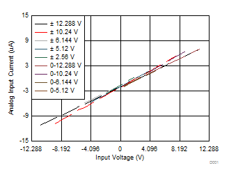
GUID-32F1C48E-A703-4E5E-A0A1-92946F66140A-low.gif
 
Figure 6-9 Input I-V Characteristic Across Input Ranges
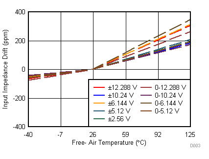
GUID-8D8DA487-DBE3-4267-BF01-3AD8CBD3A0F5-low.gif
 
Figure 6-11 Input Impedance Drift vs Temperature
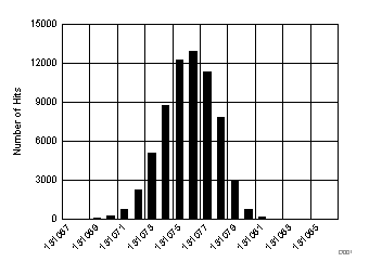
GUID-8FEECF82-9CA1-4F24-A909-9479F2D8C9B3-low.gif
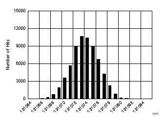
Mean = 131076.2, sigma = 1.9, input = 0 V
Figure 6-13 DC Histogram for Mid-Scale Inputs (±12.288 V)
GUID-40127870-4418-4DFB-9130-6FB641E704CD-low.gif
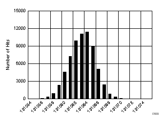
Mean = 131063.9, sigma = 2.23, input = 0 V
Figure 6-15 DC Histogram for Mid-Scale Inputs (±6.144 V)
GUID-441F2F45-4430-4BE7-8BEF-8641F06AB6B9-low.gif
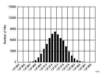
Mean = 131073, sigma = 3.24, input = 0 V
Figure 6-17 DC Histogram for Mid-Scale Inputs (±2.56 V)
GUID-ADEC42EB-9230-4256-947C-7AE06790F44D-low.gif
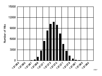
Mean = 131073.9, sigma = 2.49, input = 5.12 V
Figure 6-19 DC Histogram for Mid-Scale Inputs (0 V–10.24 V)
GUID-FC1C9E5E-C17F-4A00-B5A8-22AAE9F3990F-low.gif
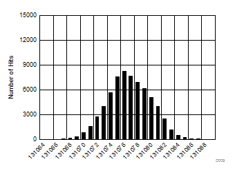
Mean = 131076.8, sigma = 3.61, input = 2.56 V
Figure 6-21 DC Histogram for Mid-Scale Inputs (0 V–5.12 V)
GUID-FA317252-E34E-434C-8915-D3A47F2983CC-low.gif
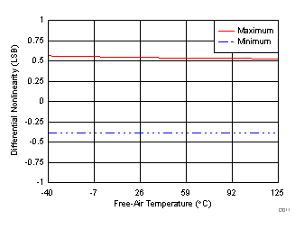
All input ranges
Figure 6-23 DNL vs Temperature
GUID-22EA8A46-EA1F-4124-B3F6-6A5FE519A247-low.gif
 
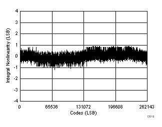
Figure 6-25 Typical INL for All Codes (All Unipolar Ranges)
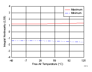
GUID-0DBD631D-B705-4B65-A893-8FC2FF12EB32-low.gif
 
Figure 6-27 INL vs Temperature (All Unipolar Ranges)
GUID-F86A5460-4597-45C1-A0A5-AF81B776955A-low.gif
 
Figure 6-29 Typical Histogram for Offset Drift
GUID-A1159B78-3ADE-405C-8BFA-A77335EAB5D8-low.gif
 
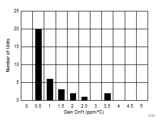
Figure 6-31 Typical Histogram for Gain Error Drift
GUID-D2B5D18D-C8A7-4058-BDE5-A2D3040E37BC-low.gif
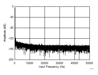
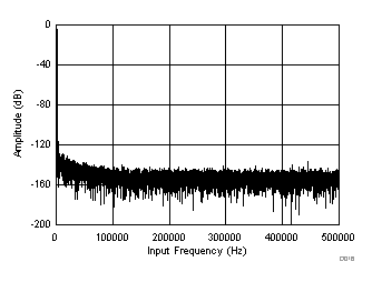
Number of points = 64k, fIN = 1 kHz
Figure 6-33 Typical FFT Plot (All Ranges) for the ADS8691
GUID-2D0467A7-20E5-4166-B691-5790CBEECB0A-low.gif
Number of points = 64k, fIN = 1 kHz
Figure 6-35 Typical FFT Plot (All Ranges) for the ADS8699
GUID-BBCA5403-065D-4B4E-B4F0-02C27B26C629-low.gif
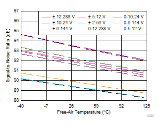
fIN = 1 kHz
Figure 6-37 SNR vs Temperature
GUID-C9C68B75-CC03-4D68-8CF4-AEA9BEAB99C4-low.gif
fIN = 1 kHz
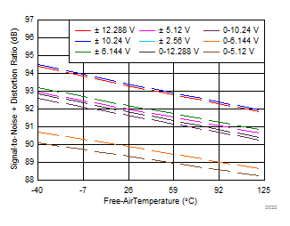
Figure 6-39 SINAD vs Temperature
GUID-BB8E01EA-ED41-47C8-973C-88D9AA3A0A09-low.gif
fIN = 1 kHz
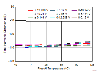
Figure 6-41 THD vs Temperature
GUID-0564D48C-501E-4D26-9E4A-422C32F94CCB-low.gif
 
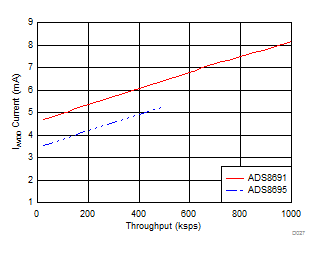
Figure 6-43 AVDD Current vs Throughput
GUID-DAFD0BD3-C57B-4187-8EBF-D613F1D93CDC-low.gif
 
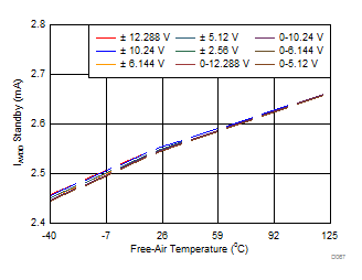
Figure 6-45 AVDD Current vs Temperature (Standby Mode)
GUID-F1365E9E-6A68-4E5D-BD30-21DA5B954031-low.gif
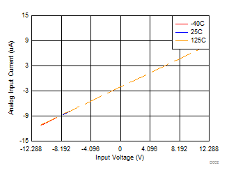
Range = ±12.288 V
Figure 6-10 Input I-V Characteristic Across Temperature
GUID-BD8889AE-CA2F-4B20-88AA-CCE3A8E808DE-low.gif
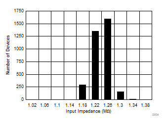
Number of samples = 3398
Figure 6-12 Typical Distribution of Input Impedance
GUID-9CB9A915-AF59-468B-B85A-386A25B3038C-low.gif
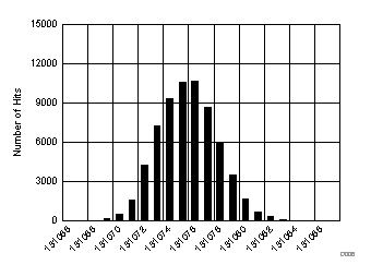
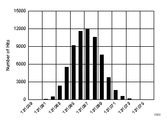
Mean = 131066.8, sigma = 2.04, input = 0 V
Figure 6-14 DC Histogram for Mid-Scale Inputs (±10.24 V)
GUID-B111A031-3833-4EE9-A7E7-2A6691A1D9E6-low.gif
Mean = 131073.5, sigma = 2.23, input = 0 V
Figure 6-16 DC Histogram for Mid-Scale Inputs (±5.12 V)
GUID-676D2A67-E97C-41EE-AE3D-79F7EF4D4C99-low.gif
Mean = 131075.5, sigma = 2.41, input = 6.144 V
Figure 6-18 DC Histogram for Mid-Scale Inputs (0 V–12.288 V)
GUID-ADB27EEE-FD7C-40C1-A253-AA9B7455046A-low.gif
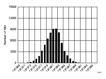
Mean = 131082, sigma = 3.17, input = 3.072 V
Figure 6-20 DC Histogram for Mid-Scale Inputs (0 V–6.144 V)
GUID-0EB48234-1BB5-46F0-B94B-EBAB50F8F8CC-low.gif
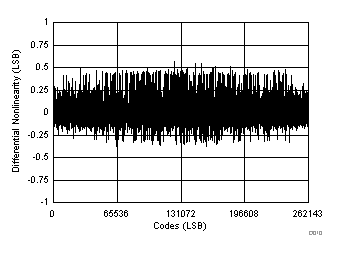
All input ranges
Figure 6-22 Typical DNL for All Codes
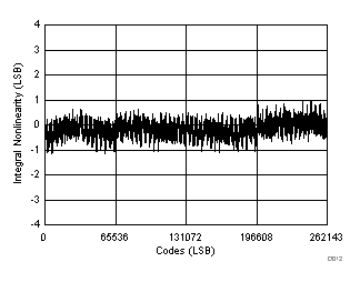
GUID-F062485A-A55C-427E-B78B-BFCD2C0864E8-low.gif
 
Figure 6-24 Typical INL for All Codes (All Bipolar Ranges)
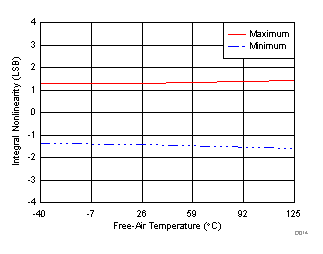
GUID-759B49B1-F205-4DB0-B699-59633ECEF4CD-low.gif
 
Figure 6-26 INL vs Temperature (All Bipolar Ranges)
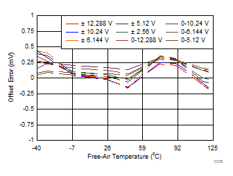
GUID-D7531B03-D790-4452-883C-348A136ADB00-low.gif
 
Figure 6-28 Offset Error vs Temperature Across Input Ranges
GUID-C89C2002-9379-4DB6-BD8A-E84D6222E926-low.gif
 
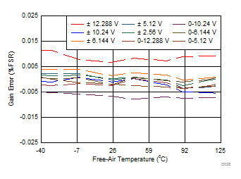
Figure 6-30 Gain Error vs Temperature Across Input Ranges
GUID-0652E860-28CD-4871-ABB8-938993305F78-low.gif
 
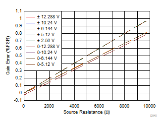
Figure 6-32 Gain Error vs External Resistance (REXT)
GUID-7201CBF6-2616-45EE-9152-9E7B21BFF048-low.gif
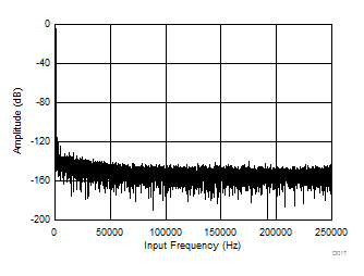
Number of points = 64k, fIN = 1 kHz
Figure 6-34 Typical FFT Plot (All Ranges) for the ADS8695
GUID-99DF63C4-ABF0-47DC-BC81-513F4A270AF9-low.gif
 
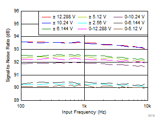
Figure 6-36 SNR vs Input Frequency
GUID-B810ABDD-982E-4CF2-905C-29414A646ABD-low.gif
 
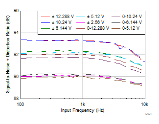
Figure 6-38 SINAD vs Input Frequency
GUID-9CD00D9E-11D3-42C6-95ED-309FE11D8511-low.gif
 
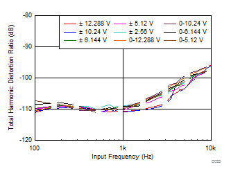
Figure 6-40 THD vs Input Frequency
GUID-59D033C3-B6DF-4981-9474-AF5444F0BC5A-low.gif
 
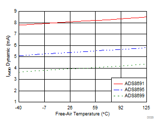
Figure 6-42 AVDD Current vs Temperature
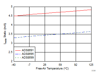
GUID-4A868A07-53B9-434D-A050-C146EEAE7606-low.gif
 
Figure 6-44 AVDD Current vs Temperature (During Sampling)
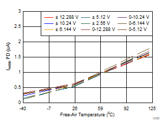
GUID-42555055-BE5E-4C47-BBA1-D2E8D18EC024-low.gif
 
Figure 6-46 AVDD Current vs Temperature (Power-Down Mode)