ZHCSBG4B May 2013 – February 2019 ADS8862
PRODUCTION DATA.
- 1 特性
- 2 应用
- 3 说明
- 4 修订历史记录
- 5 Device Comparison Table
- 6 Pin Configuration and Functions
- 7 Specifications
- 8 Parameter Measurement Information
- 9 Detailed Description
- 10Application and Implementation
- 11Power Supply Recommendations
- 12Layout
- 13器件和文档支持
- 14机械、封装和可订购信息
封装选项
机械数据 (封装 | 引脚)
散热焊盘机械数据 (封装 | 引脚)
- DRC|10
订购信息
9.3.2 Reference
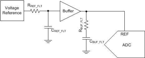
The device operates with an external reference voltage and switches binary-weighted capacitors onto the reference terminal (REF pin) during the conversion process. The switching frequency is proportional to the internal conversion clock frequency but the dynamic charge requirements are a function of the absolute value of the input voltage and reference voltage. This dynamic load must be supported by a reference driver circuit without degrading the noise and linearity performance of the device. During the acquisition process, the device automatically powers down and does not take any dynamic current from the external reference source. The basic circuit diagram for such a reference driver circuit for precision ADCs is shown in Figure 46; see the ADC Reference Driver section for more details on the application circuits.
 Figure 46. Reference Driver Schematic