ZHCSBG4B May 2013 – February 2019 ADS8862
PRODUCTION DATA.
- 1 特性
- 2 应用
- 3 说明
- 4 修订历史记录
- 5 Device Comparison Table
- 6 Pin Configuration and Functions
- 7 Specifications
- 8 Parameter Measurement Information
- 9 Detailed Description
- 10Application and Implementation
- 11Power Supply Recommendations
- 12Layout
- 13器件和文档支持
- 14机械、封装和可订购信息
封装选项
机械数据 (封装 | 引脚)
散热焊盘机械数据 (封装 | 引脚)
- DRC|10
订购信息
9.4.1.2 3-Wire CS Mode With a Busy Indicator
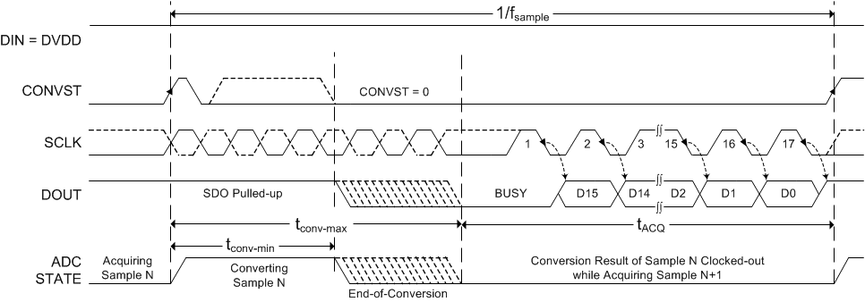
This interface option is most useful when a single ADC is connected to an SPI-compatible digital host and an interrupt-driven data transfer is desired. In this interface option, DIN can be connected to DVDD and CONVST functions as CS (as shown in Figure 50). The pull-up resistor on the DOUT pin ensures that the IRQ pin of the digital host is held high when DOUT goes to 3-state. As shown in Figure 51, a CONVST rising edge forces DOUT to 3-state, samples the input signal, and causes the device to enter a conversion phase. Conversion is done with the internal clock and continues regardless of the state of CONVST. As a result, CONVST (functioning as CS) can be pulled low after the start of the conversion to select other devices on the board. However, CONVST must be pulled low before the minimum conversion time (tconv-min) elapses and must remain low until the maximum possible conversion time (tconv-max) elapses. A low level on the CONVST input at the end of a conversion ensures the device generates a busy indicator.
 Figure 50. Connection Diagram: 3-Wire CS Mode With a Busy Indicator
  Figure 51. Interface Timing Diagram: 3-Wire CS Mode With a Busy Indicator (DIN = 1)
 When conversion is complete, the device enters an acquisition phase and powers down, DOUT comes out of 3-state, and the device outputs a busy indicator bit (low level) on the DOUT pin. This configuration provides a high-to-low transition on the IRQ pin of the digital host. The data bits are clocked out, MSB first, on the subsequent SCLK falling edges. Data can be read at either SCLK falling or rising edges. Note that with any SCLK frequency, reading data at SCLK falling edge requires the digital host to clock in the data during the th_CK_DO-min time frame. DOUT goes to 3-state after the 17th SCLK falling edge or when CONVST goes high, whichever occurs first.