ZHCSBG4B May 2013 – February 2019 ADS8862
PRODUCTION DATA.
- 1 特性
- 2 应用
- 3 说明
- 4 修订历史记录
- 5 Device Comparison Table
- 6 Pin Configuration and Functions
- 7 Specifications
- 8 Parameter Measurement Information
- 9 Detailed Description
- 10Application and Implementation
- 11Power Supply Recommendations
- 12Layout
- 13器件和文档支持
- 14机械、封装和可订购信息
封装选项
机械数据 (封装 | 引脚)
散热焊盘机械数据 (封装 | 引脚)
- DRC|10
订购信息
9.4.2.2 Daisy-Chain Mode With a Busy Indicator
This interface option is most useful in applications where multiple ADC devices are used but the digital host has limited interfacing capability and an interrupt-driven data transfer is desired. Figure 60 shows a connection diagram with N ADCs connected in the daisy-chain. The CONVST pins of all ADCs in the chain are connected together and are controlled by a single pin of the digital host. Similarly, the SCLK pins of all ADCs in the chain are connected together and are controlled by a single pin of the digital host. The DIN pin for ADC 1 (DIN-1) is connected to its CONVST. The DOUT pin of ADC 1 (DOUT-1) is connected to the DIN pin of ADC 2 (DIN-2), and so on. The DOUT pin of the last ADC in the chain (DOUT-N) is connected to the SDI and IRQ pins of the digital host.
 Figure 60. Connection Diagram: Daisy-Chain Mode With a Busy Indicator (DIN = 0)
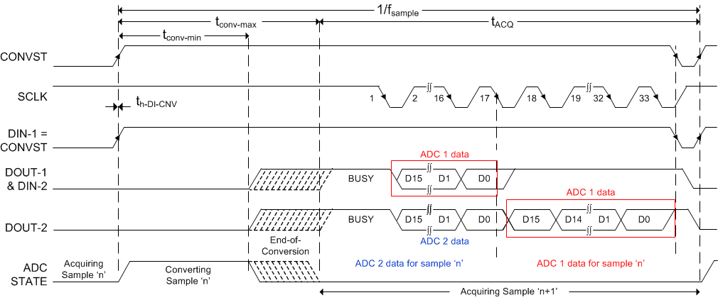
 As shown in Figure 61, the device DOUT pin is driven low when DIN and CONVST are low together. A CONVST rising edge selects daisy-chain mode, samples the analog input, and causes the device to enter a conversion phase. In this interface option, CONVST must remain high from the start of the conversion until all data bits are read. When started, the conversion continues regardless of the state of SCLK, however SCLK must be high at the CONVST rising edge so that the device generates a busy indicator at the end of the conversion.
 Figure 61. Interface Timing Diagram: For Two Devices in Daisy-Chain Mode With a Busy Indicator
 At the end of conversion, every ADC in the chain loads its own conversion result into the internal, 16-bit, shift register and also forces its DOUT pin high, thereby providing a low-to-high transition on the IRQ pin of the digital host. All ADCs enter an acquisition phase and power-down. On every subsequent SCLK falling edge, the internal shift register of each ADC latches the data available on its DIN pin and shifts out the next bit of data on its DOUT pin. Therefore, the digital host receives the interrupt signal followed by the data of ADC N followed by the data of ADC N–1, and so on (in MSB-first fashion). A total of (16 × N) + 1 SCLK falling edges are required to capture the outputs of all N devices in the chain. Data can be read at either SCLK falling or rising edges. With any SCLK frequency, reading data at the SCLK falling edge requires the digital host to clock in the data during the th_CK_DO-min time frame. The busy indicator bits of ADC 1 to ADC N–1 do not propagate to the next device in the chain.
NOTE
SPI mode-3 (CPOL = 1, CPHA = 1) allows reading the conversion results of N ADCs in 18 × N SCLK cycles because the busy indicator bit is not clocked in by the host.