ZHCSF64B June 2016 – January 2018 ADS8910B , ADS8912B , ADS8914B
PRODUCTION DATA.
- 1 特性
- 2 应用
- 3 说明
- 4 Revision History
- 5 Pin Configuration and Functions
- 6 Specifications
-
7 Detailed Description
- 7.1 Overview
- 7.2 Functional Block Diagram
- 7.3 Feature Description
- 7.4 Device Functional Modes
- 7.5
Programming
- 7.5.1 Output Data Word
- 7.5.2 Data Transfer Frame
- 7.5.3 Interleaving Conversion Cycles and Data Transfer Frames
- 7.5.4 Data Transfer Protocols
- 7.5.5 Device Setup
- 7.6
Register Maps
- 7.6.1
Device Configuration and Register Maps
- 7.6.1.1 PD_CNTL Register (address = 04h) [reset = 00h]
- 7.6.1.2 SDI_CNTL Register (address = 008h) [reset = 00h]
- 7.6.1.3 SDO_CNTL Register (address = 0Ch) [reset = 00h]
- 7.6.1.4 DATA_CNTL Register (address = 010h) [reset = 00h]
- 7.6.1.5 PATN_LSB Register (address = 014h) [reset = 00h]
- 7.6.1.6 PATN_MID Register (address = 015h) [reset = 00h]
- 7.6.1.7 PATN_MSB Register (address = 016h) [reset = 00h]
- 7.6.1.8 OFST_CAL Register (address = 020h) [reset = 00h]
- 7.6.1.9 REF_MRG Register (address = 030h) [reset = 00h]
- 7.6.1
Device Configuration and Register Maps
-
8 Application and Implementation
- 8.1 Application Information
- 8.2 Typical Application
- 9 Power-Supply Recommendations
- 10Layout
- 11器件和文档支持
- 12机械、封装和可订购信息
6.7 Switching Characteristics
At RVDD = 5.5 V, DVDD = 1.65 V to 5.5 V, VREF = 5 V, and maximum throughput (unless otherwise noted).Minimum and maximum values at TA = –40°C to +125°C; typical values at TA = 25°C.
| PARAMETER | MIN | TYP | MAX | UNIT | TIMING DIAGRAM | ||
|---|---|---|---|---|---|---|---|
| CONVERSION CYCLE | |||||||
| tconv | Conversion time | ADS8910B | 580 | 640 | ns | Figure 1 | |
| ADS8912B | 1100 | 1200 | |||||
| ADS8914B | 2400 | 2500 | |||||
| ASYNCHRONOUS RESET, AND LOW POWER MODES | |||||||
| td_rst | Delay time: RST rising to RVS rising | 3 | ms | Figure 2 | |||
| tPU_ADC | Power-up time for converter module | 1 | ms | See PD_CNTL Register | |||
| tPU_REFBUF | Power-up time for internal reference buffer, CREFBUF = 22 µF | 10 | ms | ||||
| tPU_Device | Power-up time for device | CLDO = 1 µF, CREFBUF = 22 µF | 10 | ms | |||
| SPI-COMPATIBLE SERIAL INTERFACE | |||||||
| tden_CSDO | Delay time: CS falling to data enable | 9 | ns | Figure 3 | |||
| tdz_CSDO | Delay time: CS rising to SDO going to Hi-Z | 10 | ns | ||||
| td_CKDO | Delay time: SCLK launch edge to (next) data valid on SDO | 13 | ns | ||||
| td_CSRDY_f | Delay time: CS falling to RVS falling | 12 | ns | Figure 4 | |||
| td_CSRDY_r | Delay time: CS rising to RVS rising |
After NOP operation | 30 | ns | Figure 4 | ||
| After WR or RD operation | 120 | ||||||
| SOURCE-SYNCHRONOUS SERIAL INTERFACE (External Clock)(1) | |||||||
| td_CKSTR_r | Delay time: SCLK launch edge to RVS rising | 13 | ns | Figure 4 | |||
| td_CKSTR_f | Delay time: SCLK launch edge to RVS falling | 13 | ns | ||||
| toff_STRDO_f | Time offset: RVS falling to (next) data valid on SDO | -2 | 2 | ns | |||
| toff_STRDO_r | Time offset: RVS rising to (next) data valid on SDO | -2 | 2 | ns | |||
| tph_STR | Strobe output high time, 2.35 V ≤ DVDD ≤ 5.5 V | 0.45 | 0.55 | tSTR | |||
| tpl_STR | Strobe output low time, 2.35 V ≤ DVDD ≤ 5.5 V | 0.45 | 0.55 | tSTR | |||
| SOURCE-SYNCHRONOUS SERIAL INTERFACE (Internal Clock) | |||||||
| td_CSSTR | Delay time: CS falling to RVS rising | 15 | 50 | ns | Figure 5 | ||
| tSTR | Strobe output time period | INTCLK option | 15 | ns | |||
| INTCLK / 2 option | 30 | ||||||
| INTCLK / 4 option | 60 | ||||||
| tph_STR | Strobe output high time | 0.45 | 0.55 | tSTR | |||
| tpl_STR | Strobe output low time | 0.45 | 0.55 | tSTR | |||
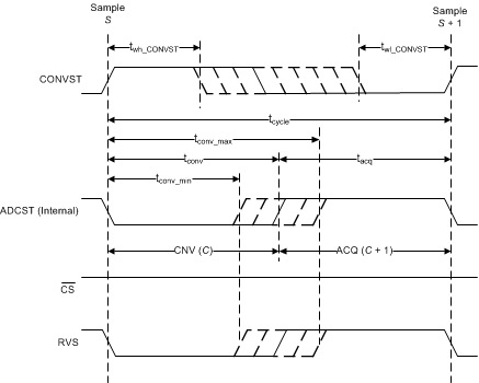 Figure 1. Conversion Cycle Timing
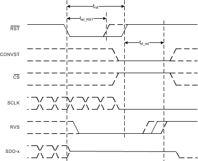 Figure 2. Asynchronous Reset Timing
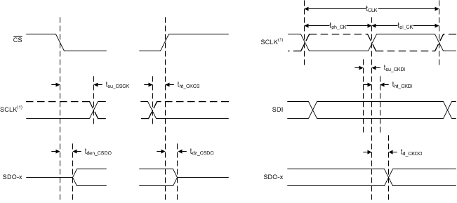
1. The SCLK polarity, launch edge, and capture edge depend on the SPI protocol selected.
Figure 3. SPI-Compatible Serial Interface Timing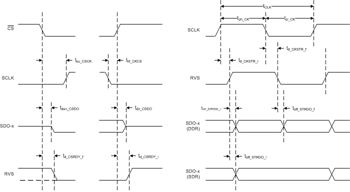 Figure 4. Source-Synchronous Serial Interface Timing (External Clock)
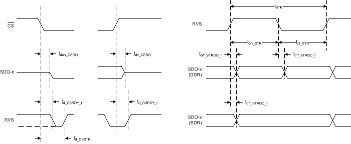 Figure 5. Source-Synchronous Serial Interface Timing (Internal Clock)