ZHCSF64B June 2016 – January 2018 ADS8910B , ADS8912B , ADS8914B
PRODUCTION DATA.
- 1 特性
- 2 应用
- 3 说明
- 4 Revision History
- 5 Pin Configuration and Functions
- 6 Specifications
-
7 Detailed Description
- 7.1 Overview
- 7.2 Functional Block Diagram
- 7.3 Feature Description
- 7.4 Device Functional Modes
- 7.5
Programming
- 7.5.1 Output Data Word
- 7.5.2 Data Transfer Frame
- 7.5.3 Interleaving Conversion Cycles and Data Transfer Frames
- 7.5.4 Data Transfer Protocols
- 7.5.5 Device Setup
- 7.6
Register Maps
- 7.6.1
Device Configuration and Register Maps
- 7.6.1.1 PD_CNTL Register (address = 04h) [reset = 00h]
- 7.6.1.2 SDI_CNTL Register (address = 008h) [reset = 00h]
- 7.6.1.3 SDO_CNTL Register (address = 0Ch) [reset = 00h]
- 7.6.1.4 DATA_CNTL Register (address = 010h) [reset = 00h]
- 7.6.1.5 PATN_LSB Register (address = 014h) [reset = 00h]
- 7.6.1.6 PATN_MID Register (address = 015h) [reset = 00h]
- 7.6.1.7 PATN_MSB Register (address = 016h) [reset = 00h]
- 7.6.1.8 OFST_CAL Register (address = 020h) [reset = 00h]
- 7.6.1.9 REF_MRG Register (address = 030h) [reset = 00h]
- 7.6.1
Device Configuration and Register Maps
-
8 Application and Implementation
- 8.1 Application Information
- 8.2 Typical Application
- 9 Power-Supply Recommendations
- 10Layout
- 11器件和文档支持
- 12机械、封装和可订购信息
7.4.1 RST State
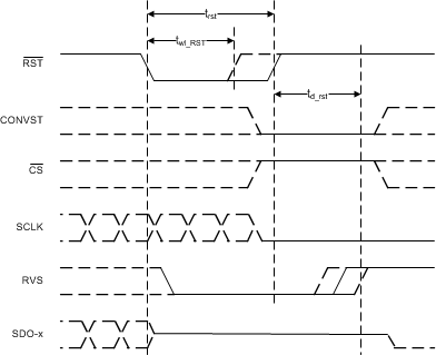
The RST pin is an asynchronous digital input for the device. To enter RST state, the host controller pulls the RST pin low and keeps it low for the twl_RST duration (as specified in the Timing Requirements table).
In RST state, all configuration registers (see the Register Maps section) are reset to their default values, the RVS pin remains low, and the SDO-x pins are Hi-Z.
To exit RST state, the host controller pulls the RST pin high, with CONVST and SCLK held low and CS held high, as shown in Figure 39. After a delay of td_rst, the device enters ACQ state and the RVS pin goes high.
 Figure 39. Asynchronous Reset
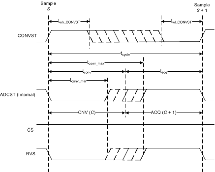
To operate the device in either ACQ or CNV state, RST must be held high. With RST held high, transitions on the CONVST pin determine the functional state of the device.
Figure 40 shows a typical conversion process. The internal ADCST signal goes low during conversion and goes high at the end of conversion. With CS held high, RVS reflects the status of ADCST.
 Figure 40. Typical Conversion Process