ZHCSF64B June 2016 – January 2018 ADS8910B , ADS8912B , ADS8914B
PRODUCTION DATA.
- 1 特性
- 2 应用
- 3 说明
- 4 Revision History
- 5 Pin Configuration and Functions
- 6 Specifications
-
7 Detailed Description
- 7.1 Overview
- 7.2 Functional Block Diagram
- 7.3 Feature Description
- 7.4 Device Functional Modes
- 7.5
Programming
- 7.5.1 Output Data Word
- 7.5.2 Data Transfer Frame
- 7.5.3 Interleaving Conversion Cycles and Data Transfer Frames
- 7.5.4 Data Transfer Protocols
- 7.5.5 Device Setup
- 7.6
Register Maps
- 7.6.1
Device Configuration and Register Maps
- 7.6.1.1 PD_CNTL Register (address = 04h) [reset = 00h]
- 7.6.1.2 SDI_CNTL Register (address = 008h) [reset = 00h]
- 7.6.1.3 SDO_CNTL Register (address = 0Ch) [reset = 00h]
- 7.6.1.4 DATA_CNTL Register (address = 010h) [reset = 00h]
- 7.6.1.5 PATN_LSB Register (address = 014h) [reset = 00h]
- 7.6.1.6 PATN_MID Register (address = 015h) [reset = 00h]
- 7.6.1.7 PATN_MSB Register (address = 016h) [reset = 00h]
- 7.6.1.8 OFST_CAL Register (address = 020h) [reset = 00h]
- 7.6.1.9 REF_MRG Register (address = 030h) [reset = 00h]
- 7.6.1
Device Configuration and Register Maps
-
8 Application and Implementation
- 8.1 Application Information
- 8.2 Typical Application
- 9 Power-Supply Recommendations
- 10Layout
- 11器件和文档支持
- 12机械、封装和可订购信息
7.5.3 Interleaving Conversion Cycles and Data Transfer Frames
The host controller operates the device at the desired throughput by interleaving the conversion cycles and the data transfer frames.
The cycle time of the device, tcycle, is the time difference between two consecutive CONVST rising edges provided by the host controller. The response time of the device, tresp, is the time difference between the host controller initiating conversion C, and the host controller receiving the complete result for conversion C.
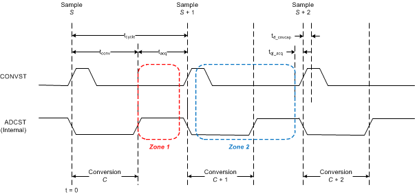
Figure 44 shows three conversion cycles: C, C + 1, and C + 2. Conversion C is initiated by a CONVST rising edge at time t = 0, and the conversion result becomes available for data transfer at tconv. However, this result is loaded into the ODR only on the subsequent CS falling edge. This CS falling edge must be provided before the completion of conversion C + 1 (that is, before tcycle + tconv).
To achieve the rated performance specifications, the host controller must make sure that no digital signals toggle during the quiet acquisition time (tqt_acq) and quiet aperture time (td_cnvcap). Any noise during td_cnvcap may negatively affect the result of the ongoing conversion, whereas any noise during tqt_acq may negatively affect the result of the subsequent conversion.
 Figure 44. Data Transfer Zones
This architecture allows for two distinct time zones (zone 1 and zone 2) to transfer data for each conversion. Zone 1 and zone 2 for conversion C are defined in Table 3.
Table 3. Data Transfer Zones Timing
| ZONE | STARTING TIME | ENDING TIME |
|---|---|---|
| Zone 1 for conversion C |  |
 |
| Zone 2 for conversion C |  |
 |
The response time includes the conversion time and the data transfer time, and thus is a function of the selected data transfer zone.
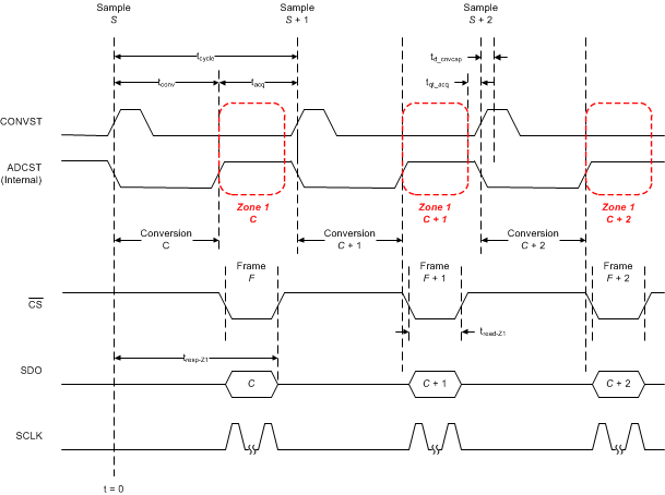
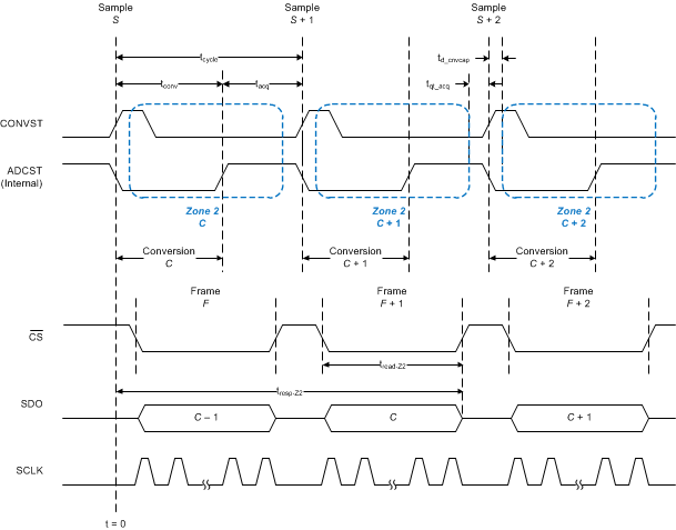
Figure 45 and Figure 46 illustrate interleaving of three conversion cycles (C, C + 1, and C + 2) with three data transfer frames (F, F + 1, and F + 2) in zone 1 and in zone 2, respectively.
 Figure 45. Zone 1 Data Transfer
 Figure 46. Zone 2 Data Transfer
To achieve cycle time tcycle, the read time in zone 1 is given by Equation 5:

For an optimal data transfer frame, Equation 5 results in an SCLK frequency given by Equation 6:

Then, the zone 1 data transfer achieves a response time defined by Equation 7:

At lower SCLK speeds, tread-Z1 increases, resulting in slower response times and higher cycle times.
To achieve the same cycle time, tcycle, the read time in zone 2 is given by Equation 8:

For an optimal data transfer frame, Equation 8 results in an SCLK frequency given by Equation 9:

Then, the zone 2 data transfer achieves a response time defined by Equation 10:

Any increase in tread-Z2 increases response time and may increase cycle time.
For a given cycle time, the zone 1 data transfer clearly achieves faster response time, but also requires a higher SCLK speed (as evident from Equation 5, Equation 6, and Equation 7); whereas, the zone 2 data transfer clearly requires a lower SCLK speed but has a slower response time (as evident from Equation 8, Equation 9, and Equation 10). For more information about benefits of zone 2 data transfer when using isolated digital interface or MCU refer to TI TechNote - Simplify Isolation Designs Using an Enhanced-SPI ADC Interface.
NOTE
A data transfer frame can begin in zone 1, and then extend into zone 2; however, the host controller must make sure that no digital transitions occur during the tqt_acq and td_cnvcap time intervals.
NOTE
For data transfer operations in zone 2 using the ADC-Clock-Master protocol
(SDO_MODE[1:0] = 11b), the device supports only the external-clock-echo option
(SSYNC_CLK_SEL[1:0] = 00b); see Table 9.