ZHCSF64B June 2016 – January 2018 ADS8910B , ADS8912B , ADS8914B
PRODUCTION DATA.
- 1 特性
- 2 应用
- 3 说明
- 4 Revision History
- 5 Pin Configuration and Functions
- 6 Specifications
-
7 Detailed Description
- 7.1 Overview
- 7.2 Functional Block Diagram
- 7.3 Feature Description
- 7.4 Device Functional Modes
- 7.5
Programming
- 7.5.1 Output Data Word
- 7.5.2 Data Transfer Frame
- 7.5.3 Interleaving Conversion Cycles and Data Transfer Frames
- 7.5.4 Data Transfer Protocols
- 7.5.5 Device Setup
- 7.6
Register Maps
- 7.6.1
Device Configuration and Register Maps
- 7.6.1.1 PD_CNTL Register (address = 04h) [reset = 00h]
- 7.6.1.2 SDI_CNTL Register (address = 008h) [reset = 00h]
- 7.6.1.3 SDO_CNTL Register (address = 0Ch) [reset = 00h]
- 7.6.1.4 DATA_CNTL Register (address = 010h) [reset = 00h]
- 7.6.1.5 PATN_LSB Register (address = 014h) [reset = 00h]
- 7.6.1.6 PATN_MID Register (address = 015h) [reset = 00h]
- 7.6.1.7 PATN_MSB Register (address = 016h) [reset = 00h]
- 7.6.1.8 OFST_CAL Register (address = 020h) [reset = 00h]
- 7.6.1.9 REF_MRG Register (address = 030h) [reset = 00h]
- 7.6.1
Device Configuration and Register Maps
-
8 Application and Implementation
- 8.1 Application Information
- 8.2 Typical Application
- 9 Power-Supply Recommendations
- 10Layout
- 11器件和文档支持
- 12机械、封装和可订购信息
7.5.1 Output Data Word
In any data transfer frame, the contents of an internal, 22-bit, output data word are shifted out on the SDO pins. The D[21:4] bits of the 22-bit output data word for any frame F + 1, are determined by:
- Value of the DATA_VAL bit applicable to frame F + 1 (see the DATA_CNTL register)
- The command issued in frame F
If a valid RD_REG command is executed in frame F, then the D[21:14] bits in frame F + 1 reflect the contents of the selected register, and the D[13:0] bits are zeros.
If the DATA_VAL bit for frame F + 1 is set to 1, then the D[21:4] bits in frame F + 1 are replaced by the DATA_PATN[17:0] bits.
For all other combinations, the D[21:4] bits for frame F + 1 are the latest conversion result.
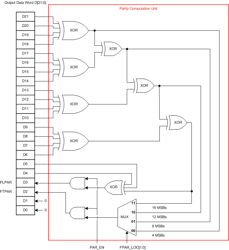
Figure 41 shows the output data word. Figure 42 shows further details of the parity computation unit illustrated in Figure 41.
![ADS8910B ADS8912B ADS8914B Output Data Word
(D[21:0]) ADS8910B ADS8912B ADS8914B ai_odw_config_18_bas707.gif](/ods/images/ZHCSF64B/ai_odw_config_18_bas707.gif) Figure 41. Output Data Word (D[21:0])
Figure 41. Output Data Word (D[21:0]) Figure 42. Parity Bits Computation
With the PAR_EN bit set to 0, the D[3] and D[2] bits of the output data word are set to 0 (default configuration).
When the PAR_EN bit is set to 1, the device calculates the parity bits (FLPAR and FTPAR) and appends them as bits D[3] and D[2].
- FLPAR is the even parity calculated on bits D[21:4].
- FTPAR is the even parity calculated on the bits defined by FPAR_LOC[1:0].
See the DATA_CNTL register for more details on the FPAR_LOC[1:0] bit settings. Bits D[1:0] are set to 00b.