ZHCSF64B June 2016 – January 2018 ADS8910B , ADS8912B , ADS8914B
PRODUCTION DATA.
- 1 特性
- 2 应用
- 3 说明
- 4 Revision History
- 5 Pin Configuration and Functions
- 6 Specifications
-
7 Detailed Description
- 7.1 Overview
- 7.2 Functional Block Diagram
- 7.3 Feature Description
- 7.4 Device Functional Modes
- 7.5
Programming
- 7.5.1 Output Data Word
- 7.5.2 Data Transfer Frame
- 7.5.3 Interleaving Conversion Cycles and Data Transfer Frames
- 7.5.4 Data Transfer Protocols
- 7.5.5 Device Setup
- 7.6
Register Maps
- 7.6.1
Device Configuration and Register Maps
- 7.6.1.1 PD_CNTL Register (address = 04h) [reset = 00h]
- 7.6.1.2 SDI_CNTL Register (address = 008h) [reset = 00h]
- 7.6.1.3 SDO_CNTL Register (address = 0Ch) [reset = 00h]
- 7.6.1.4 DATA_CNTL Register (address = 010h) [reset = 00h]
- 7.6.1.5 PATN_LSB Register (address = 014h) [reset = 00h]
- 7.6.1.6 PATN_MID Register (address = 015h) [reset = 00h]
- 7.6.1.7 PATN_MSB Register (address = 016h) [reset = 00h]
- 7.6.1.8 OFST_CAL Register (address = 020h) [reset = 00h]
- 7.6.1.9 REF_MRG Register (address = 030h) [reset = 00h]
- 7.6.1
Device Configuration and Register Maps
-
8 Application and Implementation
- 8.1 Application Information
- 8.2 Typical Application
- 9 Power-Supply Recommendations
- 10Layout
- 11器件和文档支持
- 12机械、封装和可订购信息
7.5.4 Data Transfer Protocols
This device family features a multiSPI digital interface that allows the host controller to operate at slower SCLK speeds and still achieve the required throughput and response time. The multiSPI digital interface module offers three options to reduce the SCLK speed required for data transfer:
- Increase the width of the output data bus.
- Enable double data rate (DDR) transfer.
- Extended data transfer window, as shown in Figure 46.
These three options can be combined to achieve further reduction in SCLK speed.
There are various factors that limit the maximum SCLK frequency in a system.
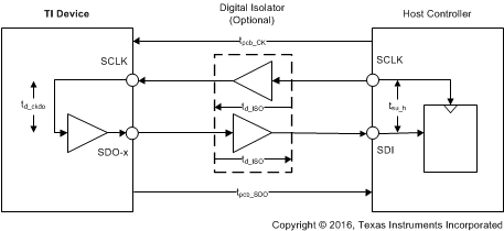
Figure 47 shows the delays in the communication channel between the host controller and the device in a typical serial communication.
 Figure 47. Delays in Serial Communication
For example, if tpcb_CK and tpcb_SDO are the delays introduced by the printed circuit board (PCB) traces for the serial clock and SDO signals, td_CKDO is the clock-to-data delay of the device, td_ISO is the propagation delay introduced by the digital isolator, and tsu_h is the setup time specification of the host controller, then the total delay in the path is given by Equation 11:

In a standard SPI protocol, the host controller and the device launch and capture data bits on alternate SCLK edges. Therefore, the td_total_serial delay must be kept to less than half of the SCLK duration. Equation 12 shows the fastest clock allowed by the SPI protocol:

Larger values of the td_total_serial delay restricts the maximum SCLK speed for the SPI protocol, resulting in higher read and response times, and can possibly limit the throughput.
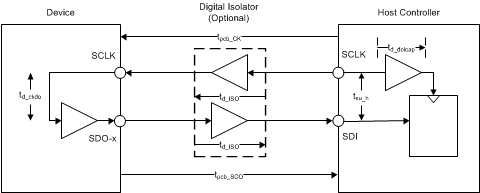
Figure 48 shows a delay (td_delcap) introduced in the capture path (inside the host controller).
 Figure 48. Delayed Capture
The total delay in the path modifies to Equation 13:

This reduction in total delay allows the SPI protocol to operate at higher clock speeds.
The multiSPI digital interface module offers two additional options to remove the restriction on the SCLK speed:
- Early data launch (EDL) mode of operation
- ADC-Clock-Master (source-synchronous) mode of operation
In EDL mode, the device launches the output data on SDO-x pin (or pins) half a clock earlier compared to the standard SPI protocol. Therefore, Equation 12 modifies to Equation 14:

The reduction in total delay allows the serial interface to operate at higher clock speeds.
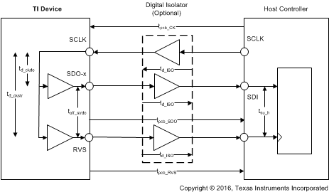
As illustrated in Figure 49, in ADC-Clock-Master mode, the device provides a synchronous output clock (on the RVS pin) along with the output data (on the SDO-x pins).
 Figure 49. Delays in ADC-Clock-Master (Source-Synchronous) Mode
For negligible values of toff_STRDO, the total delay in the path for a source-synchronous data transfer, is given by Equation 15:

As shown by the difference between Equation 11 and Equation 15, using ADC-Clock-Master mode completely eliminates the effect of isolator delays (td_ISO) and clock-to-data delays (td_CKDO); typically, the largest contributors in the overall delay computation.
Furthermore, the actual values of tpcb_RVS and tpcb_SDO do not matter. In most cases, the td_total_srcsync delay can be kept at a minimum by routing the RVS and SDO lines together on the PCB. Therefore, the ADC-Clock-Master mode allows the data transfer between the host controller and the device to operate at much higher SCLK speeds. For more information about using ADC-Clock-Master to mode to achieve fast SCLK speeds, with an isolated interface or high routing delays, see Optimizing Data Transfer on High-Resolution, High Throughput Data Converters. Zone 2 data transfer also enables longer quiet time for analog input settling, and is discussed in Improving Input Settling for Precision Data Converters.