ZHCSFE1B June 2016 – August 2017 ADS8920B , ADS8922B , ADS8924B
PRODUCTION DATA.
- 1 特性
- 2 应用
- 3 说明
- 4 Revision History
- 5 Pin Configuration and Functions
- 6 Specifications
-
7 Detailed Description
- 7.1 Overview
- 7.2 Functional Block Diagram
- 7.3 Feature Description
- 7.4 Device Functional Modes
- 7.5
Programming
- 7.5.1 Output Data Word
- 7.5.2 Data Transfer Frame
- 7.5.3 Interleaving Conversion Cycles and Data Transfer Frames
- 7.5.4 Data Transfer Protocols
- 7.5.5 Device Setup
- 7.6
Register Maps
- 7.6.1
Device Configuration and Register Maps
- 7.6.1.1 PD_CNTL Register (address = 04h) [reset = 00h]
- 7.6.1.2 SDI_CNTL Register (address = 008h) [reset = 00h]
- 7.6.1.3 SDO_CNTL Register (address = 0Ch) [reset = 00h]
- 7.6.1.4 DATA_CNTL Register (address = 010h) [reset = 00h]
- 7.6.1.5 PATN_LSB Register (address = 014h) [reset = 00h]
- 7.6.1.6 PATN_MID Register (address = 015h) [reset = 00h]
- 7.6.1.7 PATN_MSB Register (address = 016h) [reset = 00h]
- 7.6.1.8 OFST_CAL Register (address = 020h) [reset = 00h]
- 7.6.1.9 REF_MRG Register (address = 030h) [reset = 00h]
- 7.6.1
Device Configuration and Register Maps
-
8 Application and Implementation
- 8.1 Application Information
- 8.2 Typical Application
- 9 Power-Supply Recommendations
- 10Layout
- 11器件和文档支持
- 12机械、封装和可订购信息
7.5.4.2.2 SPI-Compatible Protocols with Bus Width Options
The device provides an option to increase the SDO bus width from one bit (default, single SDO) to two bits (dual SDO) or four bits (quad SDO) when operating with any of the four legacy, SPI-compatible protocols.
Set the SDO_WIDTH[1:0] bits in the SDO_CNTL register to select the SDO bus width. The SCLK launch edge depends on the SPI protocol selection (as shown in Table 7).
Table 7. SPI-Compatible Protocols with Bus Width Options
| PROTOCOL | SCLK POLARITY (At CS Falling Edge) | SCLK PHASE (Capture Edge) | MSB BIT LAUNCH EDGE | SDI_CNTL | SDO_CNTL | #SCLK (Optimal Read Frame) | TIMING DIAGRAM |
|---|---|---|---|---|---|---|---|
| SPI-00-D | Low | Rising | CS falling | 00h | 08h | 8 | Figure 62 |
| SPI-01-D | Low | Falling | First SCLK rising | 01h | 08h | 8 | Figure 63 |
| SPI-10-D | High | Falling | CS falling | 02h | 08h | 8 | Figure 64 |
| SPI-11-D | High | Rising | First SCLK falling | 03h | 08h | 8 | Figure 65 |
| SPI-00-Q | Low | Rising | CS falling | 00h | 0Ch | 4 | Figure 66 |
| SPI-01-Q | Low | Falling | First SCLK rising | 01h | 0Ch | 4 | Figure 67 |
| SPI-10-Q | High | Falling | CS falling | 02h | 0Ch | 4 | Figure 68 |
| SPI-11-Q | High | Rising | First SCLK falling | 03h | 0Ch | 4 | Figure 69 |
In dual-SDO mode (SDO_WIDTH[1:0] = 10b), two bits of data are launched on the two SDO pins (SDO-0 and SDO-1) on every SCLK launch edge.
In quad-SDO mode (SDO_WIDTH[1:0] = 11b), four bits of data are launched on the four SDO pins (SDO-0, SDO-1, SDO-2, and SDO-3) on every SCLK launch edge.
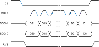 Figure 62. SPI-00-D Protocol
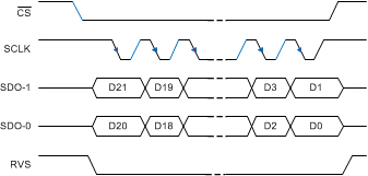 Figure 64. SPI-10-D Protocol
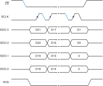 Figure 66. SPI-00-Q Protocol
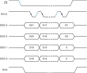 Figure 68. SPI-10-Q Protocol
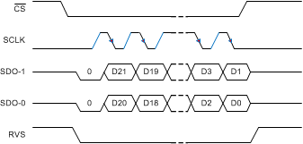 Figure 63. SPI-01-D Protocol
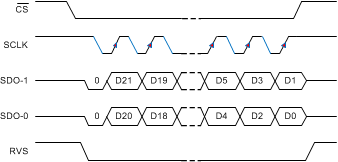 Figure 65. SPI-11-D Protocol
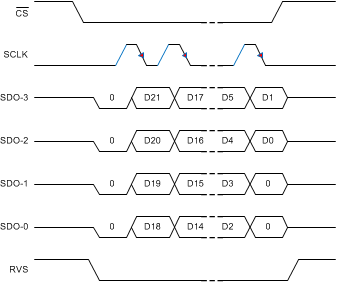 Figure 67. SPI-01-Q Protocol
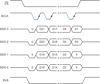 Figure 69. SPI-11-Q Protocol
For SDI_MODE[1:0] = 00b or 10b, the device supports an early data launch (EDL) option. Set SDO_MODE[1:0] = 01b in the SDO_CNTL register to enable the feature (see Table 8). Setting SDO_MODE[1:0] = 01b has no effect if SDI_MODE[1:0] = 01b or 11b.
Table 8. SPI Protocols with Early Data Launch
| PROTOCOL | SCLK POLARITY (At CS Falling Edge) | SCLK PHASE (Capture Edge) | MSB BIT LAUNCH EDGE | SDI_CNTL | SDO_CNTL | NO. OF SCLK (Optimal Read Frame) | TIMING DIAGRAM |
|---|---|---|---|---|---|---|---|
| SPI-00-D-EDL | Low | Rising | CS falling | 00h | 09h | 8 | Figure 62 |
| SPI-10-D-EDL | High | Falling | CS falling | 02h | 09h | 8 | Figure 64 |
| SPI-00-Q-EDL | Low | Rising | CS falling | 00h | 0Dh | 4 | Figure 66 |
| SPI-10-Q-EDL | High | Falling | CS falling | 02h | 0Dh | 4 | Figure 68 |
As shown in Figure 60, and Figure 61, the device launches the output data bits on the SDO-x pins half clock earlier compared to the standard SPI protocol.
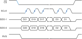 Figure 70. SPI-00-D-EDL Protocol
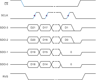 Figure 72. SPI-00-Q-EDL Protocol
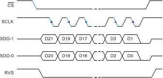 Figure 71. SPI-10-D-EDL Protocol
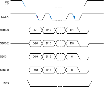 Figure 73. SPI-10-Q-EDL Protocol
When using any of the SPI-compatible protocols, the RVS output remains low throughout the data transfer frame; see the Timing Requirements and Switching Characteristics tables for associated timing parameters.
Figure 62 to Figure 73 illustrate how the wider data bus allows the host controller to read all 22 bits of the output data word using shorter data transfer frames. Table 7 and Table 8 show the number of SCLK required in an optimal read frame for the different output protocol selections.
NOTE
With SDO_CNTL[7:0] ≠ 00h or 01h, a long data transfer frame does not result in daisy-chain operation. On SDO pin (or pins), the 22 bits of output data word are followed by zeros.