ZHCSFE1B June 2016 – August 2017 ADS8920B , ADS8922B , ADS8924B
PRODUCTION DATA.
- 1 特性
- 2 应用
- 3 说明
- 4 Revision History
- 5 Pin Configuration and Functions
- 6 Specifications
-
7 Detailed Description
- 7.1 Overview
- 7.2 Functional Block Diagram
- 7.3 Feature Description
- 7.4 Device Functional Modes
- 7.5
Programming
- 7.5.1 Output Data Word
- 7.5.2 Data Transfer Frame
- 7.5.3 Interleaving Conversion Cycles and Data Transfer Frames
- 7.5.4 Data Transfer Protocols
- 7.5.5 Device Setup
- 7.6
Register Maps
- 7.6.1
Device Configuration and Register Maps
- 7.6.1.1 PD_CNTL Register (address = 04h) [reset = 00h]
- 7.6.1.2 SDI_CNTL Register (address = 008h) [reset = 00h]
- 7.6.1.3 SDO_CNTL Register (address = 0Ch) [reset = 00h]
- 7.6.1.4 DATA_CNTL Register (address = 010h) [reset = 00h]
- 7.6.1.5 PATN_LSB Register (address = 014h) [reset = 00h]
- 7.6.1.6 PATN_MID Register (address = 015h) [reset = 00h]
- 7.6.1.7 PATN_MSB Register (address = 016h) [reset = 00h]
- 7.6.1.8 OFST_CAL Register (address = 020h) [reset = 00h]
- 7.6.1.9 REF_MRG Register (address = 030h) [reset = 00h]
- 7.6.1
Device Configuration and Register Maps
-
8 Application and Implementation
- 8.1 Application Information
- 8.2 Typical Application
- 9 Power-Supply Recommendations
- 10Layout
- 11器件和文档支持
- 12机械、封装和可订购信息
8.1.2.1 Charge-Kickback Filter
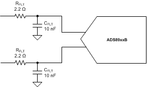
The charge-kickback filter is an RC filter at the input pins of the ADC that filters the broadband noise from the front-end drive circuitry, and attenuates the sampling charge injection from the switched-capacitor input stage of the ADC. A filter capacitor, CFLT, is connected from each input pin of the ADC to the ground (as shown in Figure 104). This capacitor helps reduce the sampling charge injection and provides a charge bucket to quickly charge the internal sample-and-hold capacitors during the acquisition process. Generally, the value of this capacitor must be at least 20 times the specified value of the ADC sampling capacitance. For the ADS892xB, the input sampling capacitance is equal to 60 pF; therefore, for optimal performance, keep CFLT greater than 1.2 nF. This capacitor must be a COG- or NPO-type. The type of dielectric used in COG or NPO ceramic capacitors provides the most stable electrical properties over voltage, frequency, and temperature changes.
 Figure 104. Charge Kickback Filter Configuration
Driving capacitive loads can degrade the phase margin of the input amplifier, thus making the amplifier marginally unstable. To avoid amplifier stability issues, series isolation resistors (RFLT) are used at the output of the amplifiers. A higher value of RFLT helps with amplifier stability, but adds distortion as a result of interactions with the nonlinear input impedance of the ADC. Distortion increases with source impedance, input signal frequency, and input signal amplitude. Therefore, the selection of RFLT requires balancing the stability of the driver amplifier and distortion performance of the design. Always verify the stability and settling behavior of the driving amplifier and charge-kickback filter by TINA-TI™ SPICE simulation. Keep the tolerance of the selected resistors less than 1% to keep the inputs balanced.