ZHCSFE1B June   2016  – August 2017 ADS8920B , ADS8922B , ADS8924B

PRODUCTION DATA.  

  1. 特性
  2. 应用
  3. 说明
    1.     Device Images
      1.      使用 ADS89xxB 集成功能轻松实现 系统设计
  4. Revision History
  5. Pin Configuration and Functions
    1.     Pin Functions
  6. Specifications
    1. 6.1 Absolute Maximum Ratings
    2. 6.2 ESD Ratings
    3. 6.3 Recommended Operating Conditions
    4. 6.4 Thermal Information
    5. 6.5 Electrical Characteristics
    6. 6.6 Timing Requirements
    7. 6.7 Switching Characteristics
    8. 6.8 Typical Characteristics
  7. Detailed Description
    1. 7.1 Overview
    2. 7.2 Functional Block Diagram
    3. 7.3 Feature Description
      1. 7.3.1 LDO Module
      2. 7.3.2 Reference Buffer Module
      3. 7.3.3 Converter Module
        1. 7.3.3.1 Sample-and-Hold Circuit
        2. 7.3.3.2 Internal Oscillator
        3. 7.3.3.3 ADC Transfer Function
      4. 7.3.4 Interface Module
    4. 7.4 Device Functional Modes
      1. 7.4.1 RST State
      2. 7.4.2 ACQ State
      3. 7.4.3 CNV State
    5. 7.5 Programming
      1. 7.5.1 Output Data Word
      2. 7.5.2 Data Transfer Frame
      3. 7.5.3 Interleaving Conversion Cycles and Data Transfer Frames
      4. 7.5.4 Data Transfer Protocols
        1. 7.5.4.1 Protocols for Configuring the Device
        2. 7.5.4.2 Protocols for Reading From the Device
          1. 7.5.4.2.1 Legacy, SPI-Compatible (SYS-xy-S) Protocols
          2. 7.5.4.2.2 SPI-Compatible Protocols with Bus Width Options
          3. 7.5.4.2.3 Source-Synchronous (SRC) Protocols
            1. 7.5.4.2.3.1 Output Clock Source Options with SRC Protocols
            2. 7.5.4.2.3.2 Bus Width Options With SRC Protocols
            3. 7.5.4.2.3.3 Output Data Rate Options With SRC Protocols
      5. 7.5.5 Device Setup
        1. 7.5.5.1 Single Device: All multiSPI Options
        2. 7.5.5.2 Single Device: Minimum Pins for a Standard SPI Interface
        3. 7.5.5.3 Multiple Devices: Daisy-Chain Topology
        4. 7.5.5.4 Multiple Devices: Star Topology
    6. 7.6 Register Maps
      1. 7.6.1 Device Configuration and Register Maps
        1. 7.6.1.1 PD_CNTL Register (address = 04h) [reset = 00h]
          1. Table 11. PD_CNTL Register Field Descriptions
        2. 7.6.1.2 SDI_CNTL Register (address = 008h) [reset = 00h]
          1. Table 12. SDI_CNTL Register Field Descriptions
        3. 7.6.1.3 SDO_CNTL Register (address = 0Ch) [reset = 00h]
          1. Table 13. SDO_CNTL Register Field Descriptions
        4. 7.6.1.4 DATA_CNTL Register (address = 010h) [reset = 00h]
          1. Table 14. DATA_CNTL Register Field Descriptions
        5. 7.6.1.5 PATN_LSB Register (address = 014h) [reset = 00h]
          1. Table 15. PATN_LSB Register Field Descriptions
        6. 7.6.1.6 PATN_MID Register (address = 015h) [reset = 00h]
          1. Table 16. PATN_MID Register Field Descriptions
        7. 7.6.1.7 PATN_MSB Register (address = 016h) [reset = 00h]
          1. Table 17. PATN_MSB Register Field Descriptions
        8. 7.6.1.8 OFST_CAL Register (address = 020h) [reset = 00h]
          1. Table 18. OFST_CAL Register Field Descriptions
        9. 7.6.1.9 REF_MRG Register (address = 030h) [reset = 00h]
          1. Table 19. REF_MRG Register Field Descriptions
  8. Application and Implementation
    1. 8.1 Application Information
      1. 8.1.1 ADC Reference Driver
      2. 8.1.2 ADC Input Driver
        1. 8.1.2.1 Charge-Kickback Filter
        2. 8.1.2.2 Input Amplifier Selection
    2. 8.2 Typical Application
      1. 8.2.1 Data Acquisition (DAQ) Circuit for Lowest Distortion and Noise Performance With Differential Input
        1. 8.2.1.1 Design Requirements
        2. 8.2.1.2 Detailed Design Procedure
        3. 8.2.1.3 Application Curves
      2. 8.2.2 DAQ Circuit With FDA Input Driver and Single-Ended or Differential Input
      3. 8.2.3 Design Requirements
      4. 8.2.4 Detailed Design Procedure
      5. 8.2.5 Application Curves
  9. Power-Supply Recommendations
  10. 10Layout
    1. 10.1 Layout Guidelines
      1. 10.1.1 Signal Path
      2. 10.1.2 Grounding and PCB Stack-Up
      3. 10.1.3 Decoupling of Power Supplies
      4. 10.1.4 Reference Decoupling
      5. 10.1.5 Differential Input Decoupling
    2. 10.2 Layout Example
  11. 11器件和文档支持
    1. 11.1 Documentation Support
      1. 11.1.1 相关文档
    2. 11.2 相关链接
    3. 11.3 Receiving Notification of Documentation Updates
    4. 11.4 社区资源
    5. 11.5 商标
    6. 11.6 静电放电警告
    7. 11.7 Glossary
  12. 12机械、封装和可订购信息

封装选项

机械数据 (封装 | 引脚)
散热焊盘机械数据 (封装 | 引脚)
订购信息

Sample-and-Hold Circuit

These devices support unipolar, fully differential, analog input signals. Figure 37 shows a small-signal equivalent circuit of the sample-and-hold circuit. Each sampling switch is represented by a resistance (RS1 and RS2, typically 50 Ω) in series with an ideal switch (SW1 and SW2). The sampling capacitors, CS1 and CS2, are typically 60 pF.
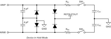
ADS8920B ADS8922B ADS8924B ai_input_sampling_sbas707.gifFigure 37. Input Sampling Stage Equivalent Circuit

During the acquisition process (ACQ state), both positive and negative inputs are individually sampled on CS1 and CS2, respectively. During the conversion process (CNV state), the device converts for the voltage difference between the two sampled values: VAINP – VAINM.

Each analog input pin has electrostatic discharge (ESD) protection diodes to REFBUFOUT and GND. Keep the analog inputs within the specified range to avoid turning the diodes on.

Equation 1 and Equation 2 show the full-scale input range (FSR) and common-mode voltage (VCM), respectively, supported at the analog inputs for any external reference voltage provided on the REFIN pin (VREF).

Equation 1. ADS8920B ADS8922B ADS8924B ai_eq_fsr_sbas629.gif
Equation 2. ADS8920B ADS8922B ADS8924B ai_eq_vcm_sbas629.gif