ZHCSFE1B June 2016 – August 2017 ADS8920B , ADS8922B , ADS8924B
PRODUCTION DATA.
- 1 特性
- 2 应用
- 3 说明
- 4 Revision History
- 5 Pin Configuration and Functions
- 6 Specifications
-
7 Detailed Description
- 7.1 Overview
- 7.2 Functional Block Diagram
- 7.3 Feature Description
- 7.4 Device Functional Modes
- 7.5
Programming
- 7.5.1 Output Data Word
- 7.5.2 Data Transfer Frame
- 7.5.3 Interleaving Conversion Cycles and Data Transfer Frames
- 7.5.4 Data Transfer Protocols
- 7.5.5 Device Setup
- 7.6
Register Maps
- 7.6.1
Device Configuration and Register Maps
- 7.6.1.1 PD_CNTL Register (address = 04h) [reset = 00h]
- 7.6.1.2 SDI_CNTL Register (address = 008h) [reset = 00h]
- 7.6.1.3 SDO_CNTL Register (address = 0Ch) [reset = 00h]
- 7.6.1.4 DATA_CNTL Register (address = 010h) [reset = 00h]
- 7.6.1.5 PATN_LSB Register (address = 014h) [reset = 00h]
- 7.6.1.6 PATN_MID Register (address = 015h) [reset = 00h]
- 7.6.1.7 PATN_MSB Register (address = 016h) [reset = 00h]
- 7.6.1.8 OFST_CAL Register (address = 020h) [reset = 00h]
- 7.6.1.9 REF_MRG Register (address = 030h) [reset = 00h]
- 7.6.1
Device Configuration and Register Maps
-
8 Application and Implementation
- 8.1 Application Information
- 8.2 Typical Application
- 9 Power-Supply Recommendations
- 10Layout
- 11器件和文档支持
- 12机械、封装和可订购信息
7.5.2 Data Transfer Frame
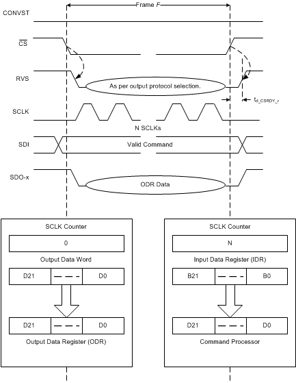
A data transfer frame between the device and the host controller is bounded between a CS falling edge and the subsequent CS rising edge. The host controller can initiate a data transfer frame (as shown in Figure 45) at any time irrespective of the status of the CONVST signal; however, the data read during such a data transfer frame is a function of relative timing between the CONVST and CS signals.
 Figure 45. Data Transfer Frame
For this discussion, assume that the CONVST signal remains low.
A typical data transfer frame F follows this order:
- The host controller pulls CS low to initiate a data transfer frame. On the CS falling edge:
- RVS goes low, indicating the beginning of the data transfer frame.
- The SCLK counter is reset to 0.
- The device takes control of the data bus. As shown in Figure 45, the 22-bit contents of the output data word (see Figure 43) are loaded in to the 22-bit output data register (ODR; see Figure 39).
- The 22-bit input data register (IDR; see Figure 39) is reset to 000000h, corresponding to a NOP command.
- During the frame, the host controller provides clocks on the SCLK pin. Inside the device:
- For each SCLK capture edge, the SCLK counter is incremented and the data bit received on the SDI pin is shifted in to the IDR.
- For each launch edge of the output clock (SCLK in this case), ODR data are shifted out on the selected SDO-x pins.
- The status of the RVS pin depends on the output protocol selection (see the Protocols for Reading From the Device section).
- The host controller pulls CS high to end the data transfer frame. On the CS rising edge:
After pulling CS high, the host controller monitors for a low-to-high transition on the RVS pin, or waits for the td_CSRDY_r time (see the Switching Characteristics table) to elapse before initiating a new operation (data transfer or conversion). The delay, td_CSRDY_r, for any data transfer frame F varies based on the data transfer operation executed in frame F.
At the end of data transfer frame F:
- If the SCLK counter is < 22, then the IDR captured less than 22 bits from the SDI. In this case, the device treats frame F as a short command frame. At the end of a short command frame, the IDR is not updated and the device treats the frame as a no operation (NOP) command.
- If the SCLK counter = 22, then the IDR captured exactly 22 bits from SDI. In this case, the device treats the frame F as a optimal command frame. At the end of an optimal command frame, the command processor decodes the 22-bit contents of the IDR as a valid command word.
- If the SCLK counter > 22, then the IDR captured more than 22 bits from the SDI; however, only the last 22 bits are retained. In this case, the device treats frame F as a long command frame. At the end of a long command frame, the command processor treats the 22-bit contents of the IDR as a valid command word. There is no restriction on the maximum number of clocks that can be provided within any data transfer frame F. However, as explained above, make sure that the last 22 bits shifted into the device before the CS rising edge constitute the desired command.
In a short command frame, the write operation to the device is invalidated; however, the output data bits transferred during the short command frame are still valid output data. Therefore, the host controller can use such shorter data transfer frames to read only the required number of MSB bits from the 22-bit output data word. As shown in Figure 43, an optimal read frame for the ADS892xB devices must read only the 16 MSB bits of the output data word. The length of an optimal read frame depends on the output protocol selection; see the Protocols for Reading From the Device section for more details.
NOTE
The previous example shows data-read and data-write operations synchronous to the external clock provided on the SCLK pin.
However, the device also supports data read operation synchronous to the internal clock; see the Protocols for Reading From the Device section for more details. In this case, while the ODR contents are shifted on the SDO (or SDOs) on the launch edge of the internal clock, the device continues to capture the SDI data into the IDR (and increment the SCLK counter) on SCLK capture edges.