ZHCSFH9 September 2016 ADS9120
PRODUCTION DATA.
- 1 特性
- 2 应用
- 3 说明
- 4 修订历史记录
- 5 Pin Configuration and Functions
-
6 Specifications
- 6.1 Absolute Maximum Ratings
- 6.2 ESD Ratings
- 6.3 Recommended Operating Conditions
- 6.4 Thermal Information
- 6.5 Electrical Characteristics
- 6.6 Timing Requirements: Conversion Cycle
- 6.7 Timing Requirements: Asynchronous Reset, NAP, and PD
- 6.8 Timing Requirements: SPI-Compatible Serial Interface
- 6.9 Timing Requirements: Source-Synchronous Serial Interface (External Clock)
- 6.10 Timing Requirements: Source-Synchronous Serial Interface (Internal Clock)
- 6.11 Typical Characteristics
-
7 Detailed Description
- 7.1 Overview
- 7.2 Functional Block Diagram
- 7.3 Feature Description
- 7.4 Device Functional Modes
- 7.5
Programming
- 7.5.1 Data Transfer Frame
- 7.5.2 Interleaving Conversion Cycles and Data Transfer Frames
- 7.5.3 Data Transfer Protocols
- 7.5.4 Device Setup
- 7.6 Register Maps
- 8 Application and Implementation
- 9 Power-Supply Recommendations
- 10Layout
- 11器件和文档支持
- 12机械、封装和可订购信息
9 Power-Supply Recommendations
The device has two separate power supplies: AVDD and DVDD. The internal circuits of the device operate on AVDD; DVDD is used for the digital interface. AVDD and DVDD can be independently set to any value within the permissible range.
9.1 Power-Supply Decoupling
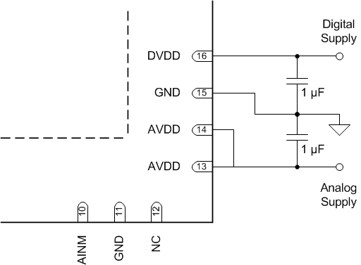
The AVDD and DVDD supply pins cannot share the same decoupling capacitor. As shown in Figure 96, separate 1-μF ceramic capacitors are recommended. These capacitors avoid digital and analog supply crosstalk resulting from dynamic currents during conversion and data transfer.
 Figure 96. Supply Decoupling
9.2 Power Saving
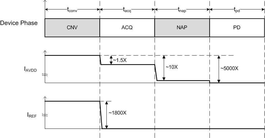
In normal mode of operation, the device does not power down between conversions, and therefore achieves a high throughput of 2.5 MSPS. However, the device offers two programmable low-power modes (NAP and PD) to reduce power consumption when the device is operated at lower throughput rates. Figure 97 shows comparative power consumption between the different modes of the device.
 Figure 97. Power Consumption in Different Operating Modes
9.2.1 NAP Mode
In NAP mode, some of the internal blocks of the device power down to reduce power consumption in the ACQ state.
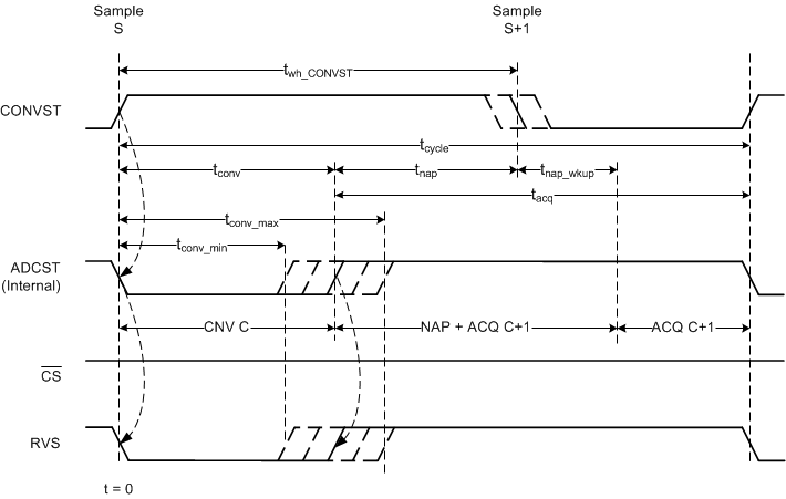
To enable NAP mode, set the NAP_EN bit in the PD_CNTL register. To exercise NAP mode, keep the CONVST pin high at the end of conversion process. The device then enters NAP mode at the end of conversion and continues in NAP mode until the CONVST pin is held high.
A CONVST falling edge brings the device out of NAP mode; however, the host controller can initiate a new conversion (CONVST rising edge) only after the tnap_wkup time has elapsed.
Figure 98 shows a typical conversion cycle with NAP mode enabled (NAP_EN = 1b).
 Figure 98. NAP Enabled Conversion Cycle
The cycle time is given by Equation 17.

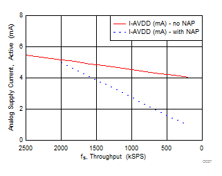
At lower throughputs, cycle time (tcycle) increases but the conversion time (tconv) remains constant, and therefore the device spends more time in NAP mode, thus giving power scaling with throughput as shown in Figure 99.
 Figure 99. Power Scaling with Throughput with NAP Mode
9.2.2 PD Mode
The device also features a deep power-down mode (PD) to reduce the power consumption at very low throughput rates.
To enter PD mode:
- Write 069h to address 011h to unlock the PD_CNTL register.
- Set the PDWN bit in the PD_CNTL register. The device enters PD mode on the CS rising edge.
In PD mode, all analog blocks within the device are powered down. All register contents are retained and the interface remains active.
To exit PD mode:
- Reset the PDWN bit in the PD_CNTL register.
- The RVS pin goes high, indicating that the device has processed the command and has started coming out of PD mode. However, the host controller must wait for the tPWRUP time to elapse before initiating a new conversion.