ZHCSFH9 September 2016 ADS9120
PRODUCTION DATA.
- 1 特性
- 2 应用
- 3 说明
- 4 修订历史记录
- 5 Pin Configuration and Functions
-
6 Specifications
- 6.1 Absolute Maximum Ratings
- 6.2 ESD Ratings
- 6.3 Recommended Operating Conditions
- 6.4 Thermal Information
- 6.5 Electrical Characteristics
- 6.6 Timing Requirements: Conversion Cycle
- 6.7 Timing Requirements: Asynchronous Reset, NAP, and PD
- 6.8 Timing Requirements: SPI-Compatible Serial Interface
- 6.9 Timing Requirements: Source-Synchronous Serial Interface (External Clock)
- 6.10 Timing Requirements: Source-Synchronous Serial Interface (Internal Clock)
- 6.11 Typical Characteristics
-
7 Detailed Description
- 7.1 Overview
- 7.2 Functional Block Diagram
- 7.3 Feature Description
- 7.4 Device Functional Modes
- 7.5
Programming
- 7.5.1 Data Transfer Frame
- 7.5.2 Interleaving Conversion Cycles and Data Transfer Frames
- 7.5.3 Data Transfer Protocols
- 7.5.4 Device Setup
- 7.6 Register Maps
- 8 Application and Implementation
- 9 Power-Supply Recommendations
- 10Layout
- 11器件和文档支持
- 12机械、封装和可订购信息
7 Detailed Description
7.1 Overview
The ADS9120 is a high-speed, successive approximation register (SAR), analog-to-digital converter (ADC) based on the charge redistribution architecture. This compact device features high performance at a high throughput rate and at low power consumption.
The ADS9120 supports unipolar, fully-differential analog input signals and operates with a 2.5-V to 5-V external reference, offering a wide selection of input ranges without additional input scaling.
When a conversion is initiated, the differential input between the AINP and AINM pins is sampled on the internal capacitor array. The ADS9120 uses an internal clock to perform conversions. During the conversion process, both analog inputs are disconnected from the internal circuit. At the end of conversion process, the device reconnects the sampling capacitors to the AINP and AINM pins and enters acquisition phase.
The device consumes only 15.5 mW of power when operating at the full 2.5-MSPS throughput. Power consumption at lower throughputs can be reduced by using the flexible low-power modes (NAP and PD).
The new multiSPI™ interface simplifies board layout, timing, and firmware, and achieves high throughput at lower clock speeds, thus allowing easy interface to a variety of microprocessors, digital signal processors (DSPs), and field-programmable gate arrays (FPGAs).
7.2 Functional Block Diagram
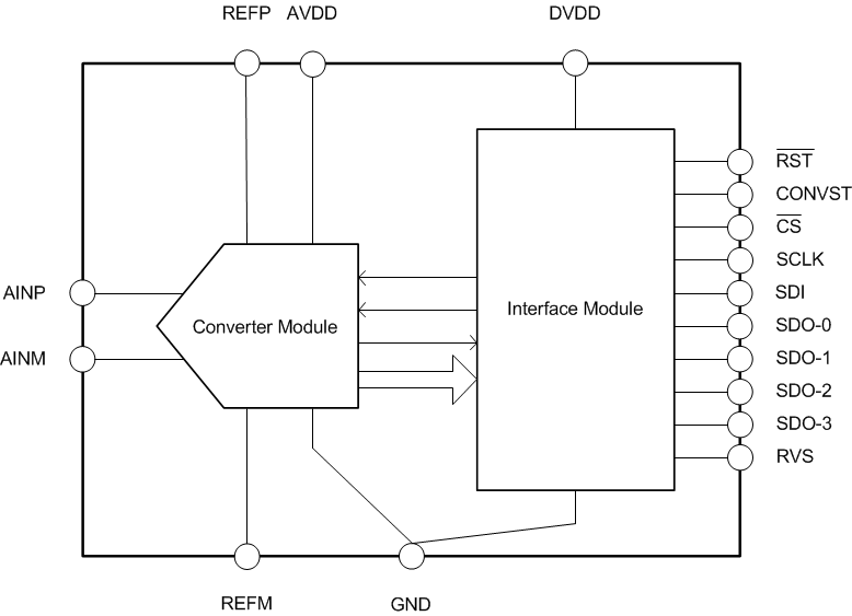
From a functional perspective, the device comprises of two modules: the converter module and the interface module, as shown in this section.
The converter module samples and converts the analog input into an equivalent digital output code whereas the interface module facilitates communication and data transfer with the host controller.
7.3 Feature Description
7.3.1 Converter Module
As shown in Figure 36, the converter module samples the analog input signal (provided between the AINP and AINM pins), compares this signal with the reference voltage (provided between the pair of REFP and REFM pins), and generates an equivalent digital output code.
The converter module receives RST and CONVST inputs from the interface module and outputs the ADCST signal and the conversion result back to the interface module.
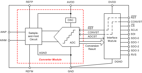 Figure 36. Converter Module
7.3.1.1 Sample-and-Hold Circuit
The device supports unipolar, fully-differential analog input signals. Figure 37 shows a small-signal equivalent circuit of the sample-and-hold circuit. Each sampling switch is represented by a resistance (Rs1 and Rs2, typically 30 Ω) in series with an ideal switch (sw1 and sw2). The sampling capacitors, Cs1 and Cs2, are typically 60 pF.
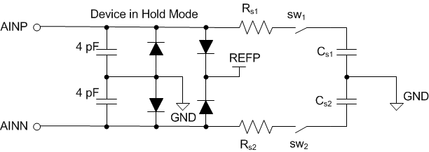 Figure 37. Input Sampling Stage Equivalent Circuit
During the acquisition process (in ACQ state), both positive and negative inputs are individually sampled on Cs1 and Cs2, respectively. During the conversion process (in CNV state), the device converts for the voltage difference between the two sampled values: VAINP – VAINM.
Each analog input pin has electrostatic discharge (ESD) protection diodes to REFP and GND. Keep the analog inputs within the specified range to avoid turning the diodes on.
Equation 1 and Equation 2 show the full-scale voltage range (FSR) and common-mode voltage range (VCM) supported at the analog inputs for any external reference voltage (VREF).


7.3.1.2 External Reference Source
The input range for the device is set by the external voltage applied at the two REFP pins. The REFM pins function as the reference ground and must be connected to each reference capacitor.
The device takes very little static current from the reference pins in the RST and ACQ states. During the conversion process (in CNV state), binary-weighted capacitors are switched onto the reference pins. The switching frequency is proportional to the conversion clock frequency, but the dynamic charge requirements are a function of the absolute values of the input voltage and the reference voltage. Reference capacitors decouple the dynamic reference loads and a low-impedance reference driver is required to keep the voltage regulated to within 1 LSB.
Most reference sources have very high broadband noise. The voltage reference source is recommended to be filtered with a 160-Hz filter before being connected to the reference driver, as shown in Figure 38. See the ADC Reference Driver section for the reference capacitor and driver selection. Also, the reference inputs are sensitive to board layout; thus, the layout guidelines described in the Layout section must be followed.
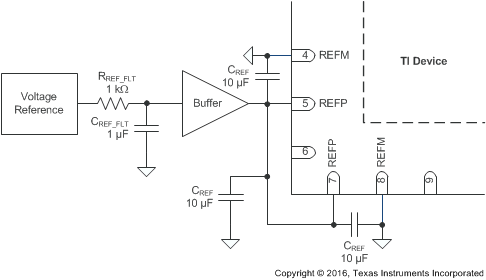 Figure 38. Reference Driver Schematic
7.3.1.3 Internal Oscillator
The device features an internal oscillator (OSC) that provides the conversion clock; see Figure 36. Conversion duration can vary but is bounded by the minimum and maximum value of tconv, as specified in the Timing Requirements: Conversion Cycle table.
The interface module can use this internal clock (OSC) or an external clock (provided by the host controller on the SCLK pin) or a combination of the internal and external clocks for executing the data transfer operations between the device and host controller; see the Interface Module section for more details.
7.3.1.4 ADC Transfer Function
The ADS9120 supports unipolar, fully-differential analog inputs. The device output is in twos compliment format. Figure 39 and Table 1 show the ideal transfer characteristics for the device.
The LSB for the ADC is given by Equation 3:

where
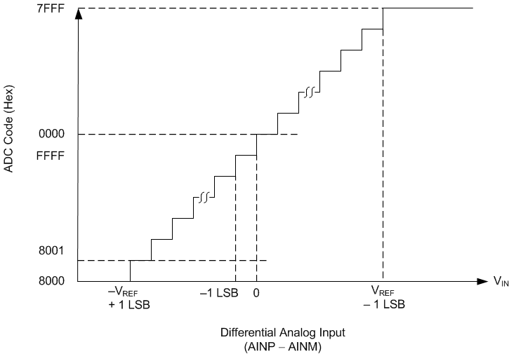 Figure 39. Differential Transfer Characteristics
Table 1. Transfer Characteristics
| DIFFERENTIAL ANALOG INPUT VOLTAGE (AINP – AINM) |
OUTPUT CODE (Hex) |
|---|---|
| < –VREF | 8000 |
| –VREF + 1 LSB | 8001 |
| –1 LSB | FFFF |
| 0 | 0000 |
| 1 LSB | 0001 |
| > VREF – 1 LSB | 7FFF |
7.3.2 Interface Module
The interface module facilitates the communication and data transfer between the device and the host controller. As shown in Figure 40, the module comprises of shift registers (both input data and output data), configuration registers, and a protocol unit.
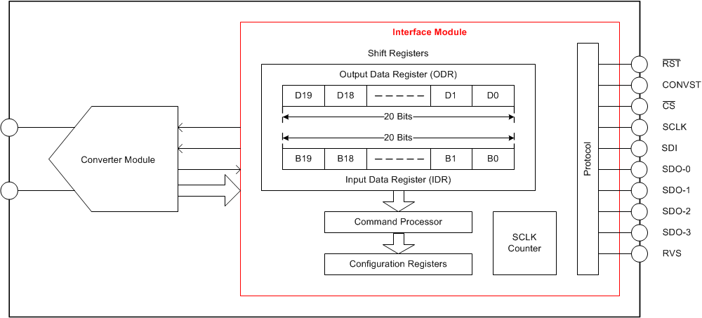 Figure 40. Interface Module
The Pin Configuration and Functions section provides descriptions of the interface pins; the Data Transfer Frame section details the functions of shift registers, the SCLK counter, and the command processor; the Data Transfer Protocols section details supported protocols; and the Register Maps section explains the configuration registers and bit settings.
7.4 Device Functional Modes
As shown in Figure 41, the device supports three functional states: RST, ACQ, and CNV. The device state is determined by the status of the CONVST and RST control signals provided by the host controller.
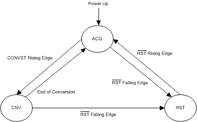 Figure 41. Device Functional States
7.4.1 RST State
In the ADS9120, the RST pin is an asynchronous digital input. To enter RST state, the host controller must pull the RST pin low and keep it low for the twl_RST duration (as specified in the Timing Requirements: Asynchronous Reset, NAP, and PD table).
In RST state, all configuration registers (see the Register Maps section) are reset to the default values, the RVS pins remain low, and the SDO-x pins are tri-stated.
To exit RST state, the host controller must pull the RST pin high with CONVST and SCLK held low and CS held high, as shown in Figure 42. After a delay of td_rst, the device enters ACQ state and the RVS pin goes high.
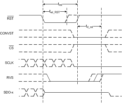 Figure 42. Asynchronous Reset
To operate the device in any of the other two states (ACQ or CNV), RST must be held high. With RST held high, transitions on the CONVST pin determine the functional state of the device.
Figure 43 shows a typical conversion process. An internal signal, ADCST, goes low during conversion and goes high at the end of conversion. With CS held high, RVS reflects the status of ADCST.
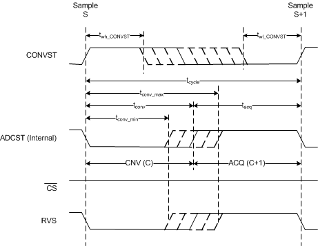 Figure 43. Typical Conversion Process
7.4.2 ACQ State
In ACQ state, the device acquires the analog input signal. The device enters ACQ state on power-up, after any asynchronous reset, or after end of every conversion.
An RST falling edge takes the device from an ACQ state to a RST state. A CONVST rising edge takes the device from an ACQ state to a CNV state.
The device offers a low-power NAP mode to reduce power consumption in the ACQ state; see the NAP Mode section for more details on NAP mode.
7.4.3 CNV State
The device moves from ACQ state to CNV state on a rising edge of the CONVST pin. The conversion process uses an internal clock and the device ignores any further transitions on the CONVST signal until the ongoing conversion is complete (that is, during the time interval of tconv).
At the end of conversion, the device enters ACQ state. The cycle time for the device is given by Equation 4:

where
NOTE
The conversion time, tconv, can vary within the specified limits of tconv_min and tconv_max (as specified in the Timing Requirements: Conversion Cycle table). After initiating a conversion, the host controller must monitor for a low-to-high transition on the RVS pin or wait for the tconv_max duration to elapse before initiating a new operation (data transfer or conversion). If RVS is not monitored, substitute tconv in Equation 4 with tconv_max.
7.5 Programming
The device features four configuration registers (as described in the Register Maps section) and supports two types of data transfer operations: data write (the host configures the device), and data read (the host reads data from the device).
To access the internal configuration registers, the device supports the commands listed in Table 2.
Table 2. Supported Commands
| OPCODE B[19:0] | COMMAND ACRONYM | COMMAND DESCRIPTION |
|---|---|---|
| 0000_0000_0000_0000_0000 | NOP | No operation |
| 1001_<8-bit address>_0000_0000 | RD_REG | Read contents from the <8-bit address> |
| 1010_<8-bit address>_<8-bit data> | WR_REG | Write <8-bit data> to the <8-bit address> |
| 1111_1111_1111_1111_1111 | NOP | No operation |
| Remaining combinations | Reserved | These commands are reserved and treated by the device as no operation |
In the ADS9120, any data write to the device is always synchronous to the external clock provided on the SCLK pin. The data read from the device can be synchronized to the same external clock or to an internal clock of the device by programming the configuration registers (see the Data Transfer Protocols section for details).
In any data transfer frame, the contents of an internal, 20-bit, output data word are shifted out on the SDO pins. The D[19:4] bits of the 20-bit output data word for any frame (F+1), are determined by the:
- Settings of the DATA_PATN[2:0] bits applicable to frame F+1 (see the DATA_CNTL register) and
- Command issued in frame F
If a valid RD_REG command is executed in frame F, then the D[19:12] bits in frame F+1 reflect the contents of the selected register and the D[11:0] bits are 0s.
If the DATA_PATN[2:0] bits for frame F+1 are set to 1xxb, then the D[19:4] bits in frame F+1 are the fixed data pattern shown in Figure 44.
For all other combinations, the D[19:4] bits for frame F+1 are the latest conversion result.
![ADS9120 Output Data Word
(D[19:0]) ADS9120 ai_odw_config_sbas710.gif](/ods/images/ZHCSFH9/ai_odw_config_sbas710.gif) Figure 44. Output Data Word (D[19:0])
Figure 44. Output Data Word (D[19:0])
Figure 45 shows further details of the parity computation unit illustrated in Figure 44.
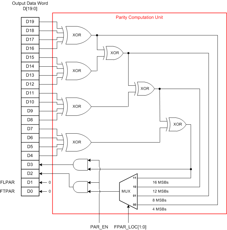 Figure 45. Parity Bits Computation
With the PAR_EN bit set to 0, the D[3] and D[2] bits of the output data word are set to 0 (default configuration).
When the PAR_EN bit is set to 1, the device calculates the parity bits (FLPAR and FTPAR) and appends them as bits D[3] and D[2].
- FLPAR is the even parity calculated on bits D[19:4].
- FTPAR is the even parity calculated on the bits defined by FPAR_LOC[1:0].
See the DATA_CNTL register for more details on the FPAR_LOC[1:0] bit settings.
The D[1] and D[0] bits are always set to 0.
7.5.1 Data Transfer Frame
A data transfer frame between the device and the host controller is bounded between a CS falling edge and the subsequent CS rising edge. The host controller can initiate a data transfer frame (as shown in Figure 46) at any time irrespective of the status of the CONVST signal; however, the data read during such a data transfer frame is a function of relative timing between the CONVST and CS signals.
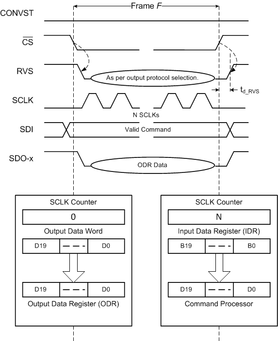 Figure 46. Data Transfer Frame
For this discussion, assume that the CONVST signal remains low.
For a typical data transfer frame F:
- The host controller pulls CS low to initiate a data transfer frame. On the CS falling edge:
- RVS goes low, indicating the beginning of the data transfer frame.
- The SCLK counter is reset to 0.
- The device takes control of the data bus. As shown in Figure 46, the 20-bit contents of the output data word (see Figure 44) are loaded in to the 20-bit ODR (see Figure 40).
- The 20-bit IDR (see Figure 40) is reset to 00000h, corresponding to a NOP command.
- During the frame, the host controller provides clocks on the SCLK pin:
- On each SCLK capture edge, the SCLK counter is incremented and the data bit received on the SDI pin is shifted in to the IDR.
- On each launch edge of the output clock (SCLK in this case), ODR data are shifted out on the selected SDO-x pins.
- The status of the RVS pin depends on the output protocol selection (see the Protocols for Reading From the Device section).
- The host controller pulls CS high to end the data transfer frame. On the CS rising edge:
After pulling CS high, the host controller must monitor for a low-to-high transition on the RVS pin or wait for the td_RVS time (see the Timing Requirements: SPI-Compatible Serial Interface table) to elapse before initiating a new operation (data transfer or conversion). The delay, td_RVS, for any data transfer frame F varies based on the data transfer operation executed in the frame F.
At the end of the data transfer frame F:
- If the SCLK counter is < 20, it indicates that IDR has captured less than 20 bits from the SDI. In this case, the device treats the frame F as a short command frame. At the end of a short command frame frame, IDR is not updated and the device treats the frame as a no operation command.
- If the SCLK counter = 20, it indicates that the IDR has captured exactly 20 bits from SDI. In this case, the device treats the frame F as a optimal command frame. At the end of an optimal command frame, the command processor decodes the 20-bit contents of the IDR as a valid command word.
- If the SCLK counter > 20, it indicates that the IDR captured more than 20 bits from the SDI, and only the last 20 bits have been retained. In this case, the device treats the frame F as a long command frame. At the end of a long command frame, the command processor treats the 20-bit contents of the IDR as a valid command word. There is no restriction on the maximum number of clocks that can be provided within any data transfer frame F. However, as explained above, the last 20 bits shifted into the device prior to the CS rising edge must constitute the desired command.
In a short command frame, the write operation to the device is invalidated, however, the output data bits transferred during the frame are still valid output data. Therefore, the host controller can use such shorter data transfer frames to read only the required number of MSB bits from the 20-bit output data word. As shown in Figure 44, an optimal read frame for ADS9120 needs to read only the 16 MSB bits of the output data word. The length of an optimal read frame depends on the output protocol selection; refer to the Protocols for Reading From the Device section for more details.
NOTE
The example above shows data read and data write operations synchronous to the external clock provided on the SCLK pin.
The device also supports data read operation synchronous to the internal clock; see the Protocols for Reading From the Device section for more details. In this case, while the ODR contents are shifted on the SDO(s) on the launch edge of the internal clock, the device continues to capture the SDI data into IDR (and increment the SCLK counter) on SCLK capture edges.
7.5.2 Interleaving Conversion Cycles and Data Transfer Frames
The host controller can operate the ADS9120 at the desired throughput by interleaving the conversion cycles and the data transfer frames.
The cycle time of the device, tcycle, is the time difference between two consecutive CONVST rising edges provided by the host controller. The response time of the device, tresp, is the time difference between the host controller initiating a conversion C and the host controller receiving the complete result for conversion C.
Figure 47 shows three conversion cycles, C, C+1, and C+2. Conversion C is initiated by a CONVST rising edge at the t = 0 time and the conversion result becomes available for data transfer at the tconv time. However, this result is loaded into the ODR only on the subsequent CS falling edge. This CS falling edge must be provided before the completion of the conversion C+1 (that is, before the tcycle + tconv time).
To achieve the rated performance specifications, the host controller must ensure that no digital signals toggle during the quiet acquisition time (tqt_acq) and quiet aperture time (td_cnvcap), as shown in Figure 47. Any noise during td_cnvcap can negatively affect the result of the ongoing conversion whereas any noise during tqt_acq can negatively affect the acquisition of the subsequent sample (and hence it's conversion result).
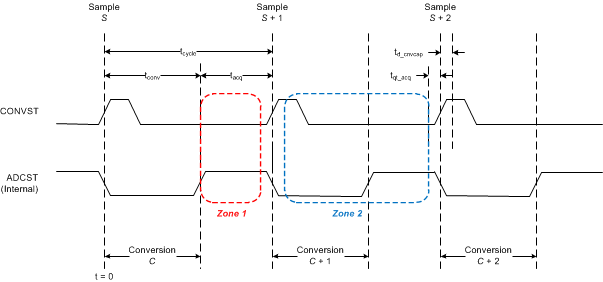 Figure 47. Data Transfer Zones
This architecture allows for two distinct time zones (zone1 and zone2) to transfer data for each conversion. Zone1 and zone2 for conversion C are defined in Table 3.
Table 3. Data Transfer Zones Timing
| ZONE | STARTING TIME | ENDING TIME |
|---|---|---|
| Zone1 for conversion C |  |
 |
| Zone2 for conversion C |  |
 |
The response time includes the conversion time and the data transfer time, and is thus a function of the data transfer zone selected.
Figure 48 and Figure 49 illustrate interleaving of three conversion cycles (C, C+1, and C+2) with three data transfer frames (F, F+1, and F+2) in zone1 and in zone2, respectively.
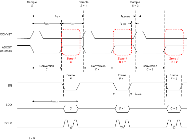 Figure 48. Zone1 Data Transfer
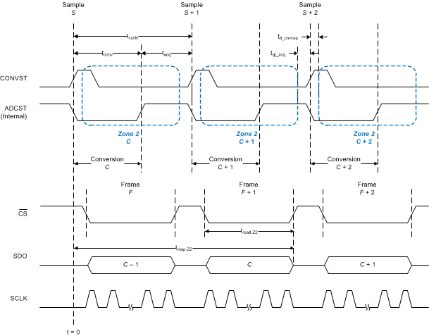 Figure 49. Zone2 Data Transfer
To achieve cycle time, tcycle, the read time in zone1 is given by Equation 5:

For an optimal read frame, Equation 5 results in an SCLK frequency given by Equation 6:

Then, the zone1 data transfer achieves a response time defined by Equation 7:

As an example, when operating the ADS9120 at the full throughput of 2.5 MSPS, the host controller can achieve a response time of 400 ns provided that the data transfer in zone1 is completed within 85 ns. However, to achieve this response time, the SCLK frequency must be greater than 188 MHz.
Note that the device does not support such high SCLK speeds.
Data transfer in zone2 can acheive lower SCLK speeds for the same cycle time. The read time in zone2 is given by Equation 8:

For an optimal data transfer frame, Equation 8 results in an SCLK frequency given by Equation 9:

Then, the zone2 data transfer achieves a response time defined by Equation 10:

As an example, the host controller can operate the ADS9120 at the full throughput of 2.5 MSPS using zone2 data transfer with a 44 MHz SCLK (and a read time of 365 ns). However, zone2 data transfer results in a response time of nearly 800 ns.
There is no upper limit on tread-Z1 and tread-Z2, however, any increase in these read times will increase the response time and may increase the cycle time.
For a given cycle time, the zone1 data transfer clearly achieves faster response time but also requires a higher SCLK speed (as evident from Equation 5, Equation 6, and Equation 7), whereas the zone2 data transfer clearly requires a lower SCLK speed but supports slower response time (as evident from Equation 8, Equation 9, and Equation 10).
NOTE
In zone2, the data transfer is active when the device is converting for the next analog sample. This digital activity can interfere with the ongoing conversion and cause some degradation in SNR performance.
Additionally, a data transfer frame can begin in zone1 and then extend into zone2; however, the host controller must ensure that no digital transitions occur during the tqt_acq and td_cnvcap time intervals.
7.5.3 Data Transfer Protocols
The device features a multiSPI™ interface that allows the host controller to operate at slower SCLK speeds and still achieve the required cycle time with a faster response time. The multiSPI™ interface module offers two options to reduce the SCLK speed required for data transfer:
- An option to increase the width of the output data bus
- An option to enable double data rate (DDR) transfer
These two options can be combined to achieve further reduction in SCLK speed.
Figure 50 shows the delays between the host controller and the device in a typical serial communication.
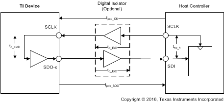 Figure 50. Delays in Serial Communication
If tpcb_CK and tpcb_SDO are the delays introduced by the PCB traces for the serial clock and SDO signals, td_CKDO is the clock-to-data delay of the device, td_ISO is the propagation delay introduced by the digital isolator, and tsu_h is the set up time specification of the host controller, then the total delay in the path is given by Equation 11:

In a standard SPI protocol, the host controller and the device launch and capture data bits on alternate SCLK edges. Therefore, the td_total_serial delay must be kept less than half of the SCLK duration. Equation 12 shows the fastest clock allowed by the SPI protocol.

Larger values of the td_total_serial delay restrict the maximum SCLK speed for the SPI protocol, resulting in higher read and response times, and can increase cycle times. To remove this restriction on the SCLK speed, the multiSPI™ interface module supports an ADC-Clock-Master or a source-synchronous mode of operation.
As illustrated in Figure 51, in the ADC-Clock-Master or source-synchronous mode, the device provides a synchronous output clock (on the RVS pin) along with the output data (on the SDO-x pins).
For negligible values of toff_STRDO, the total delay in the path for a source-synchronous data transfer, is given by Equation 13:

As illustrated in Equation 11 and Equation 13, the ADC-Clock-Master or source-synchronous mode completely eliminates the affect of isolator delays (td_ISO) and the clock-to-data delays (td_CKDO), which are typically the largest contributors in the overall delay computation.
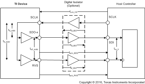 Figure 51. Delays in Source-Synchronous Communication
Furthermore, the actual values of tpcb_RVS and tpcb_SDO do not matter. In most cases, the td_total_srcsync delay can be kept at a minimum by routing the RVS and SDO lines together on the PCB. Therefore, the ADC-Clock-Master or source-synchronous mode allows the data transfer between the host controller and the device to operate at much higher SCLK speeds.
7.5.3.1 Protocols for Configuring the Device
As shown in Table 4, the host controller can use any of the four legacy, SPI-compatible protocols (SPI-00-S,
SPI-01-S, SPI-10-S, or SPI-11-S) to write data in to the device.
Table 4. SPI Protocols for Configuring the Device
| PROTOCOL | SCLK POLARITY (At CS Falling Edge) |
SCLK PHASE (Capture Edge) |
SDI_CNTL | SDO_CNTL | #SCLK (Optimal Command Frame) |
DIAGRAM |
|---|---|---|---|---|---|---|
| SPI-00-S | Low | Rising | 00h | 00h | 20 | Figure 52 |
| SPI-01-S | Low | Falling | 01h | 00h | 20 | Figure 53 |
| SPI-10-S | High | Falling | 02h | 00h | 20 | Figure 54 |
| SPI-11-S | High | Rising | 03h | 00h | 20 | Figure 55 |
On power-up or after coming out of any asynchronous reset, the device supports the SPI-00-S protocol for data read and data write operations.
To select a different SPI-compatible protocol, program the SDI_MODE[1:0] bits in the SDI_CNTL register. This first write operation must adhere to the SPI-00-S protocol. Any subsequent data transfer frames must adhere to the newly selected protocol.
Figure 52 to Figure 55 detail the four protocols using an optimal command frame; see the Timing Requirements: SPI-Compatible Serial Interface section for associated timing parameters.
NOTE
As explained in the Data Transfer Frame section, a valid write operation to the device requires a minimum of 20 SCLKs to be provided within a data transfer frame.
Any data write operation to the device must continue to follow the SPI-compatible protocol selected in the SDI_CNTL register, irrespective of the protocol selected for the data read operation.
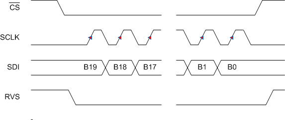 Figure 52. SPI-00-S Protocol, Optimal Command Frame
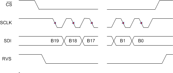 Figure 54. SPI-10-S Protocol, Optimal Command Frame
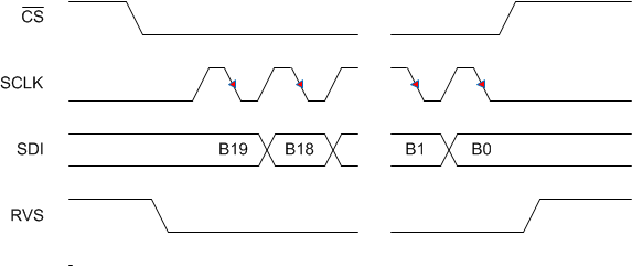 Figure 53. SPI-01-S Protocol, Optimal Command Frame
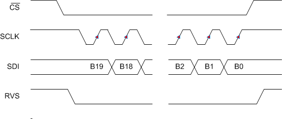 Figure 55. SPI-11-S Protocol, Optimal Command Frame
7.5.3.2 Protocols for Reading From the Device
The protocols for the data read operation can be broadly classified into three categories:
- Legacy, SPI-compatible (SPI-xy-S) protocols,
- SPI-compatible protocols with bus width options (SPI-xy-D and SPI-xy-Q), and
- Source-synchronous (SRC) protocols
7.5.3.2.1 Legacy, SPI-Compatible (SYS-xy-S) Protocols
As shown in Table 5, the host controller can use any of the four legacy, SPI-compatible protocols (SPI-00-S, SPI-01-S, SPI-10-S, or SPI-11-S) to read data from the device.
Table 5. SPI Protocols for Reading From the Device
| PROTOCOL | SCLK POLARITY (At CS Falling Edge) |
SCLK PHASE (Capture Edge) |
MSB BIT LAUNCH EDGE | SDI_CNTL | SDO_CNTL | #SCLK (Optimal Read Frame) |
DIAGRAM |
|---|---|---|---|---|---|---|---|
| SPI-00-S | Low | Rising | CS falling | 00h | 00h | 16 | Figure 56 |
| SPI-01-S | Low | Falling | 1st SCLK rising | 01h | 00h | 16 | Figure 57 |
| SPI-10-S | High | Falling | CS falling | 02h | 00h | 16 | Figure 58 |
| SPI-11-S | High | Rising | 1st SCLK falling | 03h | 00h | 16 | Figure 59 |
On power-up or after coming out of any asynchronous reset, the device supports the SPI-00-S protocol for data read and data write operations. To select a different SPI-compatible protocol for both the data transfer operations:
- Program the SDI_MODE[1:0] bits in the SDI_CNTL register. This first write operation must adhere to the SPI-00-S protocol. Any subsequent data transfer frames must adhere to the newly selected protocol.
- Set the SDO_MODE[1:0] bits = 00b in the SDO_CNTL register.
When using any of the SPI-compatible protocols, the RVS output remains low throughout the data transfer frame; see the Timing Requirements: SPI-Compatible Serial Interface table for associated timing parameters.
NOTE
It is recommended to use any of the four SPI-compatible protocols to execute the RD_REG and WR_REG operations specified in Table 2.
Figure 56 to Figure 59 explain the details of the four protocols using an optimal command frame to read all 20 bits of the output data word. Table 5 shows the number of SCLK required in an optimal read frame for the different output protocol selections.
With SDO_CNTL[7:0] = 00h, if the host controller uses a long data transfer frame, the device exhibits daisy-chain operation (see the Multiple Devices: Daisy-Chain Topology section).
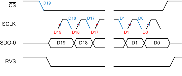 Figure 56. SPI-00-S Protocol, 20 SCLKs
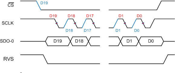 Figure 58. SPI-10-S Protocol, 20 SCLKs
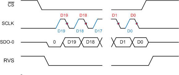 Figure 57. SPI-01-S Protocol, 20 SCLKs
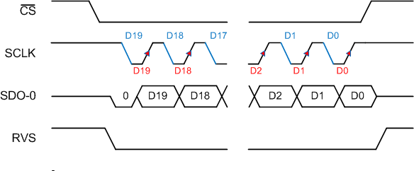 Figure 59. SPI-11-S Protocol, 20 SCLKs
7.5.3.2.2 SPI-Compatible Protocols with Bus Width Options
The device provides an option to increase the SDO bus width from one bit (default, single SDO) to two bits (dual SDO) or to four bits (quad SDO) when operating with any of the four legacy, SPI-compatible protocols.
Set the SDO_WIDTH[1:0] bits in the SDO_CNTL register to select the SDO bus width.
In dual SDO mode (SDO_WIDTH[1:0] = 10b), two bits of data are launched on the two SDO pins (SDO-0 and SDO-1) on every SCLK launch edge.
In quad SDO mode (SDO_WIDTH[1:0] = 11b), four bits of data are launched on the four SDO pins (SDO-0, SDO-1, SDO-2, and SDO-3) on every SCLK launch edge.
The SCLK launch edge depends upon the SPI protocol selection (as shown in Table 6).
Table 6. SPI-Compatible Protocols with Bus Width Options
| PROTOCOL | SCLK POLARITY (At CS Falling Edge) |
SCLK PHASE (Capture Edge) |
MSB BIT LAUNCH EDGE | SDI_CNTL | SDO_CNTL | #SCLK (Optimal Read Frame) |
DIAGRAM |
|---|---|---|---|---|---|---|---|
| SPI-00-D | Low | Rising | CS falling | 00h | 08h | 8 | Figure 60 |
| SPI-01-D | Low | Falling | First SCLK rising | 01h | 08h | 8 | Figure 61 |
| SPI-10-D | High | Falling | CS falling | 02h | 08h | 8 | Figure 62 |
| SPI-11-D | High | Rising | First SCLK falling | 03h | 08h | 8 | Figure 63 |
| SPI-00-Q | Low | Rising | CS falling | 00h | 0Ch | 4 | Figure 64 |
| SPI-01-Q | Low | Falling | First SCLK rising | 01h | 0Ch | 4 | Figure 65 |
| SPI-10-Q | High | Falling | CS falling | 02h | 0Ch | 4 | Figure 66 |
| SPI-11-Q | High | Rising | First SCLK falling | 03h | 0Ch | 4 | Figure 67 |
When using any of the SPI-compatible protocols, the RVS output remains low throughout the data transfer frame; see the Timing Requirements: SPI-Compatible Serial Interface table for associated timing parameters.
Figure 60 to Figure 67 illustrate how the wider data bus allows the host controller to read all 20 bits of the output data word using shorter data transfer frames. Table 6 shows the number of SCLK required in an optimal read frame for the different output protocol selections.
NOTE
With SDO_CNTL[7:0] ≠ 00h, a long data transfer frame does not result in daisy-chain operation. On SDO pin(s), the 20 bits of output data word are followed by 0's.
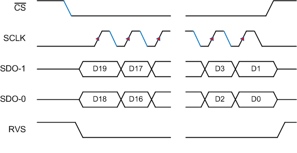 Figure 60. SPI-00-D Protocol
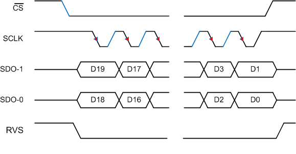 Figure 62. SPI-10-D Protocol
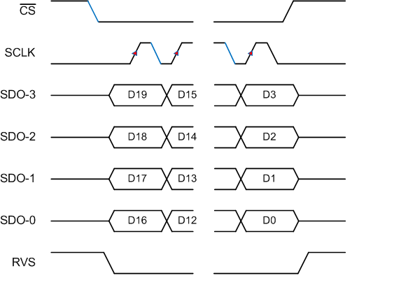 Figure 64. SPI-00-Q Protocol
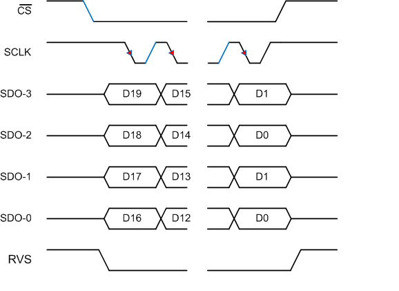 Figure 66. SPI-10-Q Protocol
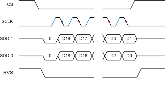 Figure 61. SPI-01-D Protocol
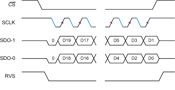 Figure 63. SPI-11-D Protocol
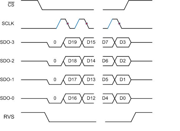 Figure 65. SPI-01-Q Protocol
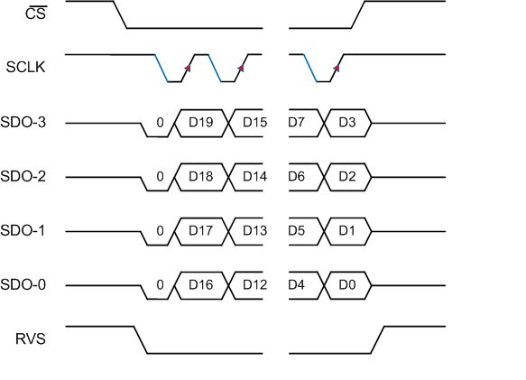 Figure 67. SPI-11-Q Protocol
7.5.3.2.3 Source-Synchronous (SRC) Protocols
As described in the Data Transfer Protocols section, the multiSPI™ interface supports an ADC-Clock-Master or a source-synchronous mode of data transfer between the device and host controller. In this mode, the device provides an output clock that is synchronous with the output data. Furthermore, the host controller can also select the output clock source, data bus width, and data transfer rate.
7.5.3.2.3.1 Output Clock Source Options with SRC Protocols
In all SRC protocols, the RVS pin provides the output clock. The device allows this output clock to be synchronous to either the external clock provided on the SCLK pin or to the internal clock of the device. Furthermore, this internal clock can be divided by a factor of two or four to lower the data rates.
As shown in Figure 68, set the SSYNC_CLK_SEL[1:0] bits in the SDO_CNTL register to select the output clock source.
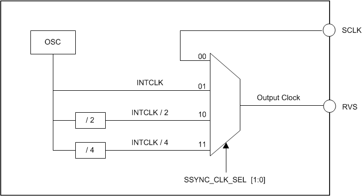 Figure 68. Output Clock Source options with SRC Protocols
7.5.3.2.3.2 Bus Width Options with SRC Protocols
The device provides an option to increase the SDO bus width from one bit (default, single SDO) to two bits (dual SDO) or to four bits (quad SDO) when operating with any of the SRC protocols. Set the SDO_WIDTH[1:0] bits in the SDO_CNTL register to select the SDO bus width.
In dual SDO mode (SDO_WIDTH[1:0] = 10b), two bits of data are launched on the two SDO pins (SDO-0 and SDO-1) on every SCLK rising edge.
In quad SDO mode (SDO_WIDTH[1:0] = 11b), four bits of data are launched on the four SDO pins (SDO-0, SDO-1, SDO-2, and SDO-3) on every SCLK rising edge.
7.5.3.2.3.3 Output Data Rate Options with SRC Protocols
The device provides an option to transfer the data to the host controller at single data rate (default, SDR) or at double data rate (DDR). Set the DATA_RATE bit in the SDO_CNTL register to select the data transfer rate.
In SDR mode (DATA_RATE = 0b), the RVS pin toggles from low to high and the output data bits are launched on the SDO pins on the output clock rising edge.
In DDR mode (DTA_RATE = 1b), the RVS pin toggles and the output data bits are launched on the SDO pins on every output clock edge, starting with the first rising edge.
The device supports all 24 combinations of output clock source, bus width, and output data rate, as shown in Table 7.
Table 7. SRC Protocol Combinations
| PROTOCOL | OUTPUT CLOCK SOURCE | BUS WIDTH | OUTPUT DATA RATE | SDI_CNTL | SDO_CNTL | #OUTPUT CLOCK (Optimal Read Frame) |
DIAGRAM |
|---|---|---|---|---|---|---|---|
| SRC-EXT-SS | SCLK | Single | SDR | 00h, 01h, 02h, or 03h |
03h | 16 | Figure 69 |
| SRC-INT-SS | INTCLK | Single | SDR | 43h | 16 | Figure 70 | |
| SRC-IB2-SS | INTCLK / 2 | Single | SDR | 83h | 16 | ||
| SRC-IB4-SS | INTCLK / 4 | Single | SDR | C3h | 16 | ||
| SRC-EXT-DS | SCLK | Dual | SDR | 0Bh | 8 | Figure 73 | |
| SRC-INT-DS | INTCLK | Dual | SDR | 4Bh | 8 | Figure 74 | |
| SRC-IB2-DS | INTCLK / 2 | Dual | SDR | 8Bh | 8 | ||
| SRC-IB4-DS | INTCLK / 4 | Dual | SDR | CBh | 8 | ||
| SRC-EXT-QS | SCLK | Quad | SDR | 0Fh | 4 | Figure 77 | |
| SRC-INT-QS | INTCLK | Quad | SDR | 4Fh | 4 | Figure 78 | |
| SRC-IB2-QS | INTCLK / 2 | Quad | SDR | 8Fh | 4 | ||
| SRC-IB4-QS | INTCLK / 4 | Quad | SDR | CFh | 4 | ||
| SRC-EXT-SD | SCLK | Single | DDR | 13h | 8 | Figure 71 | |
| SRC-INT-SD | INTCLK | Single | DDR | 53h | 8 | Figure 72 | |
| SRC-IB2-SD | INTCLK / 2 | Single | DDR | 93h | 8 | ||
| SRC-IB4-SD | INTCLK / 4 | Single | DDR | D3h | 8 | ||
| SRC-EXT-DD | SCLK | Dual | DDR | 1Bh | 4 | Figure 75 | |
| SRC-INT-DD | INTCLK | Dual | DDR | 5Bh | 4 | Figure 76 | |
| SRC-IB2-DD | INTCLK / 2 | Dual | DDR | 9Bh | 4 | ||
| SRC-IB4-DD | INTCLK / 4 | Dual | DDR | DBh | 4 | ||
| SRC-EXT-QD | SCLK | Quad | DDR | 1Fh | 2 | Figure 79 | |
| SRC-INT-QD | INTCLK | Quad | DDR | 5Fh | 2 | Figure 80 | |
| SRC-IB2-QD | INTCLK / 2 | Quad | DDR | 9Fh | 2 | ||
| SRC-IB4-QD | INTCLK / 4 | Quad | DDR | DFh | 2 |
Figure 69 to Figure 80 show the details of varoous source synchronous protocols. Table 7 shows the number of output clocks required in an optimal read frame for the different output protocol selections.
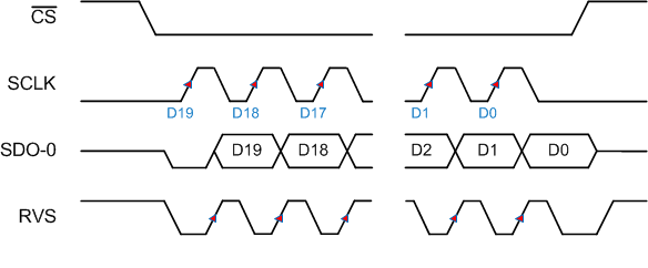 Figure 69. SRC-EXT-SS: SRC, SCLK, Single SDO, SDR
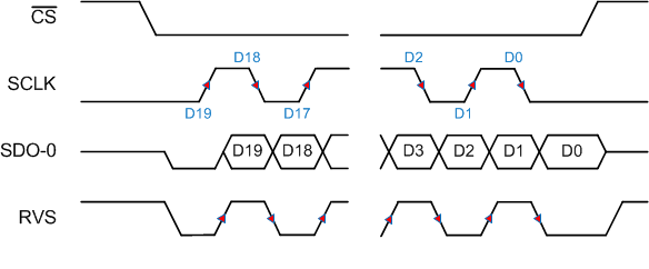 Figure 71. SRC-EXT-SD: SRC, SCLK, Single SDO, DDR
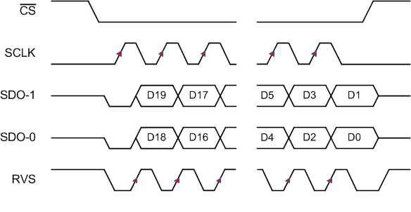 Figure 73. SRC-EXT-DS: SRC, SCLK, Dual SDO, SDR
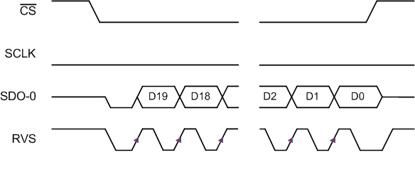 Figure 70. SRC-INT-SS: SRC, INTCLK, Single SDO, SDR
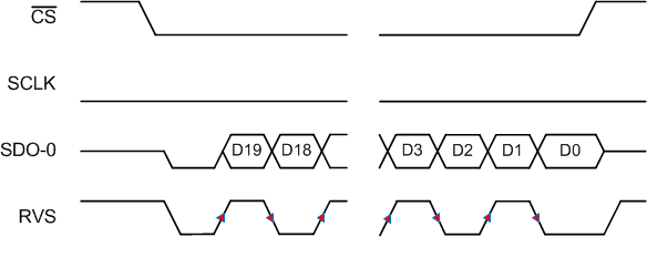 Figure 72. SRC-INT-SD: SRC, INTCLK, Single SDO, DDR
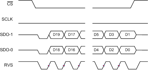 Figure 74. SRC-INT-DS: SRC, INTCLK, Dual SDO, SDR
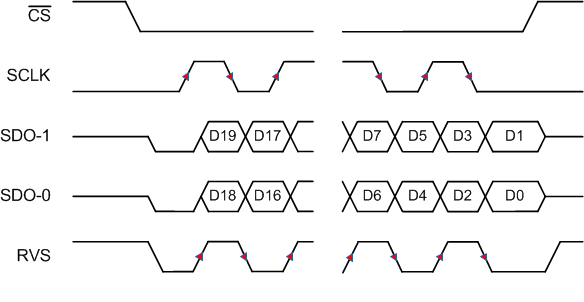 Figure 75. SRC-EXT-DD: SRC, SCLK, Dual SDO, DDR
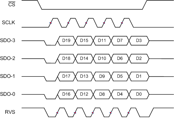 Figure 77. SRC-EXT-QS: SRC, SCLK, Quad SDO, SDR
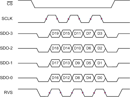 Figure 79. SRC-EXT-QD: SRC, SCLK, Quad SDO, DDR
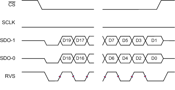 Figure 76. SRC-INT-DD: SRC, INTCLK, Dual SDO, DDR
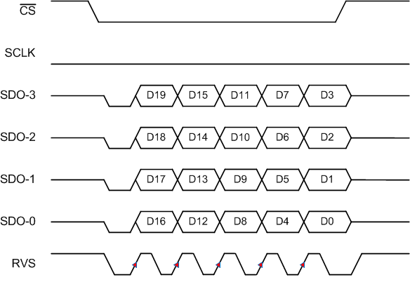 Figure 78. SRC-INT-QS: SRC, INTCLK, Quad SDO, SDR
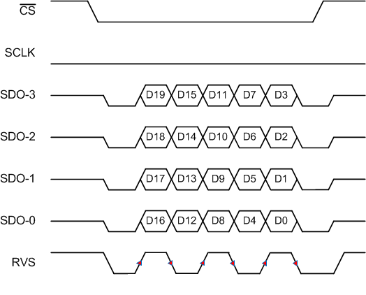 Figure 80. SRC-INT-QD: SRC, INTCLK, Quad SDO, DDR
7.5.4 Device Setup
The multiSPI™ interface and the device configuration registers offer multiple operation modes. This section describes how to select the hardware connection topology to meet different system requirements.
7.5.4.1 Single Device: All multiSPI™ Options
Figure 81 shows the connections between a host controller and a stand-alone device to exercise all options provided by the multiSPI™ interface.
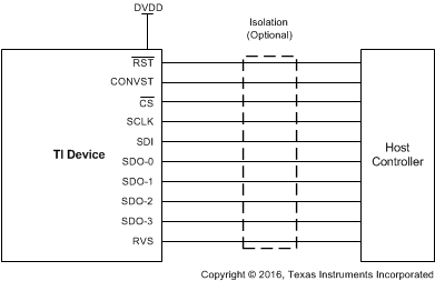 Figure 81. multiSPI™ Interface, All Pins
7.5.4.2 Single Device: Minimum Pins for a Standard SPI Interface
Figure 82 shows the minimum-pin interface for applications using a standard SPI protocol.
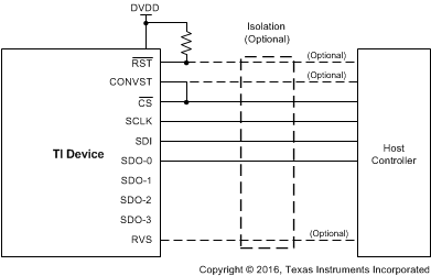 Figure 82. SPI Interface, Minimum Pins
The CS, SCLK, SDI, and SDO-0 pins constitute a standard SPI port of the host controller. The CONVST pin can be tied to CS, or can be controlled independently for additional timing flexibility. The RST pin can be tied to DVDD. The RVS pin can be monitored for timing benefits. The SDO-1, SDO-2, and SDO-3 pins have no external connections.
7.5.4.3 Multiple Devices: Daisy-Chain Topology
A typical connection diagram showing multiple devices in a daisy-chain topology is shown in Figure 83.
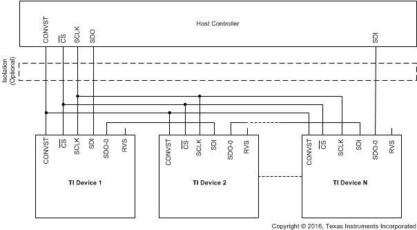 Figure 83. Daisy-Chain Connection Schematic
The CONVST, CS, and SCLK inputs of all devices are connected together and controlled by a single CONVST, CS, and SCLK pin of the host controller, respectively. The SDI input pin of the first device in the chain (device 1) is connected to the SDO pin of the host controller, the SDO-0 output pin of device 1 is connected to the SDI input pin of device 2, and so forth. The SDO-0 output pin of the last device in the chain (device N) is connected to the SDI pin of the host controller.
To operate multiple devices in a daisy-chain topology, the host controller must program the configuration registers in each device with identical values and must operate with any of the legacy, SPI-compatible protocols for data read and data write operations (SDO_CNT[7:0] = 00h). With these configurations settings, the 20-bit ODR and 20-bit IDR registers in each device collapse to form a single, 20-bit unified shift register (USR) per device, as shown in Figure 84.
 Figure 84. Unified Shift Register
All devices in the daisy-chain topology sample their analog input signals on the CONVST rising edge. The data transfer frame starts with a CS falling edge. On each SCLK launch edge, every device in the chain shifts out the MSB of its USR on to its SDO-0 pin. On every SCLK capture edge, each device in the chain shifts in data received on its SDI pin as the LSB bit of its USR. Therefore, in a daisy-chain configuration, the host controller receives the data of device N, followed by the data of device N-1, and so forth (in MSB-first fashion). On the CS rising edge, each device decodes the contents in its USR and takes appropriate action.
A typical timing diagram for three devices connected in daisy-chain topology and using the SPI-00-S protocol is shown in Figure 85.
 Figure 85. Three Devices in Daisy-Chain Mode Timing Diagram
Note that the overall throughput of the system is proportionally reduced with the number of devices connected in a daisy-chain topology.
WARNING
For N devices connected in daisy-chain topology, an optimal command frame must contain 20 × N SCLK capture edges. For a longer data transfer frame (number of SCLK in the frame > 20 x N), the host controller must appropriately align the configuration data for each device before bringing CS high. A shorter data transfer frame (number of SCLK in the frame < 20 x N) can result in an erroneous device configuration, and must be avoided.
7.5.4.4 Multiple Devices: Star Topology
A typical connection diagram showing multiple devices in the star topology is shown in Figure 86. The CONVST, SDI, and SCLK inputs of all devices are connected together and are controlled by a single CONVST, SDO, and SCLK pin of the host controller, respectively. Similarly, the SDO output pin of all devices are tied together and connected to the a single SDI input pin of the host controller. The CS input pin of each device is individually controlled by separate CS control lines from the host controller.
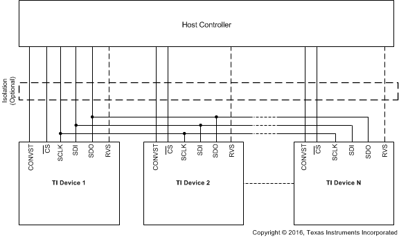 Figure 86. Star Topology Connection
The timing diagram for N devices connected in the star topology is shown in Figure 87. In order to avoid any conflict related to multiple devices driving the SDO line at the same time, ensure that the host controller pulls down the CS signal for only one device at any particular time.
 Figure 87. Three Devices Connected in Star Connection Timing Diagram
7.6 Register Maps
7.6.1 Device Configuration and Register Maps
The device features four configuration registers, mapped as described in Table 8.
Table 8. Configuration Registers Mapping
| ADDRESS | REGISTER NAME | REGISTER FUNCTION | SECTION |
|---|---|---|---|
| 010h | PD_CNTL | Low-power modes control register | PD Control |
| 014h | SDI_CNTL | SDI input protocol selection register | SDI Control |
| 018h | SDO_CNTL | SDO output protocol selection register | SDO Control |
| 01Ch | DATA_CNTL | Output data word configuration register | DATA Control |
7.6.1.1 PD_CNTL Register (address = 010h)
This register controls the low-power modes offered by the device and is protected using a key.
Any writes to the PD_CNTL register must be preceded by a write operation with the register address set to 011h and the register data set to 69h.
| 7 | 6 | 5 | 4 | 3 | 2 | 1 | 0 |
| 0 | 0 | 0 | 0 | 0 | 0 | NAP_EN | PDWN |
| R-0b | R-0b | R-0b | R-0b | R-0b | R-0b | R/W-0b | R/W-0b |
| LEGEND: R/W = Read/Write; R = Read only; -n = value after reset |
Table 9. PD_CNTL Register Field Descriptions
| Bit | Field | Type | Reset | Description |
|---|---|---|---|---|
| 7-2 | 0 | R | 000000b | Reserved bits. Reads return 000000b. |
| 1 | NAP_EN | R/W | 0b | This bit enables NAP mode for the device. 0b = NAP mode is disabled 1b = NAP mode is enabled |
| 0 | PDWN | R/W | 0b | This bit outputs the device in power-down mode. 0b = Device is powered up 1b = Device is powered down |
7.6.1.2 SDI_CNTL Register (address = 014h)
This register configures the protocol used for writing data into the device.
| 7 | 6 | 5 | 4 | 3 | 2 | 1 | 0 |
| 0 | 0 | 0 | 0 | 0 | 0 | SDI_MODE[1:0] | |
| R-0b | R-0b | R-0b | R-0b | R-0b | R-0b | R/W-0b | |
| LEGEND: R/W = Read/Write; R = Read only; -n = value after reset |
Table 10. SDI_CNTL Register Field Descriptions
| Bit | Field | Type | Reset | Description |
|---|---|---|---|---|
| 7-2 | 0 | R | 000000b | Reserved bits. Reads return 000000b. |
| 1-0 | SDI_MODE[1:0] | R/W | 00b | These bits select the protocol for writing data into the device. 00b = Standard SPI with CPOL = 0 and CPHASE = 0 01b = Standard SPI with CPOL = 0 and CPHASE = 1 10b = Standard SPI with CPOL = 1 and CPHASE = 0 11b = Standard SPI with CPOL = 1 and CPHASE = 1 |
7.6.1.3 SDO_CNTL Register (address = 018h)
This register configures the protocol for reading data from the device.
| 7 | 6 | 5 | 4 | 3 | 2 | 1 | 0 |
| SSYNC_CLK_SEL[1:0] | 0 | DATA_RATE | SDO_WIDTH[1:0] | SDO_MODE[1:0] | |||
| R/W-00b | R-0b | R/W-0b | R/W-00b | R/W-00b | |||
| LEGEND: R/W = Read/Write; R = Read only; -n = value after reset |
Table 11. SDO_CNTL Register Field Descriptions
| Bit | Field | Type | Reset | Description |
|---|---|---|---|---|
| 7-6 | SSYNC_CLK_SEL[1:0] | R/W | 00b | These bits select the source and frequency of the clock for the source-synchronous data transmission and are valid only if SDO_MODE[1:0] = 11b. 00b = External SCLK echo 01b = Internal clock (INTCLK) 10b = Internal clock / 2 (INTCLK / 2) 11b = Internal clock / 4 (INTCLK / 4) |
| 5 | 0 | R | 0b | This bit must be always set to 0. |
| 4 | DATA_RATE | R/W | 0b | This bit is ignored if SDO_MODE[1:0] = 00b. When SDO_MODE[1:0] = 11b: 0b = SDOs are updated at single data rate (SDR) with respect to the output clock 1b = SDOs are updated at double data rate (DDR) with respect to the output clock |
| 3-2 | SDO_WIDTH[1:0] | R/W | 00b | These bits set the width of the output bus. 0xb = Data are output only on SDO-0 10b = Data are output only on SDO-0 and SDO-1 11b = Data are output on SDO-0, SDO-1, SDO-2, and SDO-3 |
| 1-0 | SDO_MODE[1:0] | R/W | 00b | These bits select the protocol for reading data from the device. 00b = SDO follows the same SPI protocol as SDI; see the SDI_CNTL register 01b = Invalid configuration, not supported by the device 10b = Invalid configuration, not supported by the device 11b = SDO follows the source-synchronous protocol |
7.6.1.4 DATA_CNTL Register (address = 01Ch)
This register configures the contents of the 20-bit output data word (D[19:0]).
| 7 | 6 | 5 | 4 | 3 | 2 | 1 | 0 |
| 0 | 0 | FPAR_LOC 0 | PAR_EN | DATA_PATN[2:0] | |||
| R-0b | R-0b | R/W-00b | R/W-0b | R/W-000b | |||
| LEGEND: R/W = Read/Write; R = Read only; -n = value after reset |
Table 12. DATA_CNTL Register Field Descriptions
| Bit | Field | Type | Reset | Description |
|---|---|---|---|---|
| 7-6 | 0 | R | 00b | Reserved bits. Reads return 00b. |
| 5-4 | FPAR_LOC[1:0] | R/W | 00b | These bits control the data span for calculating the FTPAR bit (bit D[0] in the output data word). 00b = D[2] reflects even parity calculated for 4 MSB bits 01b = D[2] reflects even parity calculated for 8 MSB bits 10b = D[2] reflects even parity calculated for 12 MSB bits 11b = D[2] reflects even parity calculated for all 16 bits; that is, same as FLPAR |
| 3 | PAR_EN | R/W | 0b | 0b = Output data does not contain any parity information spaceD[3] = 0 spaceD[2] = 0 1b = Parity information is appended to the LSB of the output data spaceD[3] = Even parity calculated on bits D[19:4] spaceD[2] = Even parity computed on the selected number of MSB bits of D[19:4] as per the FPAR_LOC[1:0] setting See Figure 45 for further details of parity computation. |
| 2-0 | DATA_PATN[2:0] | R/W | 000b | These bits control bits D[19:4] of the output data word. 0xxb = 16-bit conversion output 100b = All 0s 101b = All 1s 110b = Alternating 0s and 1s (that is, 5555h) 111b = Alternating 00s and 11s (that is, 3333h) See Figure 46 for more details. |