ZHCSIJ5C August 2018 – June 2019 ADS9224R , ADS9234R
PRODUCTION DATA.
- 1 特性
- 2 应用
- 3 说明
- 4 修订历史记录
- 5 Pin Configuration and Functions
-
6 Specifications
- 6.1 Absolute Maximum Ratings
- 6.2 ESD Ratings
- 6.3 Recommended Operating Conditions
- 6.4 Thermal Information
- 6.5 Electrical Characteristics: ADS92x4R
- 6.6 Electrical Characteristics: ADS9224R
- 6.7 Electrical Characteristics: ADS9234R
- 6.8 Timing Requirements
- 6.9 Switching Characteristics
- 6.10 Typical Characteristics: ADS9224R
- 6.11 Typical Characteristics: ADS9234R
-
7 Detailed Description
- 7.1 Overview
- 7.2 Functional Block Diagram
- 7.3 Feature Description
- 7.4 Device Functional Modes
- 7.5 READY/STROBE Output
- 7.6
Programming
- 7.6.1 Output Data Word
- 7.6.2
Data Transfer Protocols
- 7.6.2.1
Protocols for Reading From the Device
- 7.6.2.1.1 Legacy, SPI-Compatible Protocols (SPI-xy-S-SDR)
- 7.6.2.1.2 SPI-Compatible Protocols With Bus Width Options and Single Data Rate (SPI-xy-D-SDR and SPI-xy-Q-SDR)
- 7.6.2.1.3 SPI-Compatible Protocols With Bus Width Options and Double Data Rate (SPI-x1-S-DDR, SPI-x1-D-DDR, SPI-x1-Q-DDR)
- 7.6.2.1.4 Clock Re-Timer (CRT) Protocols (CRT-S-SDR, CRT-D-SDR, CRT-Q-SDR, CRT-S-DDR, CRT-D-DDR, CRT-Q-DDR)
- 7.6.2.1.5 Parallel Byte Protocols (PB-xy-AB-SDR, PB-xy-AA-SDR)
- 7.6.2.2 Device Setup
- 7.6.2.3 Protocols for Configuring the Device
- 7.6.2.1
Protocols for Reading From the Device
- 7.6.3 Reading and Writing Registers
- 7.7
Register Maps
- 7.7.1
ADS92x4R Registers
- 7.7.1.1 DEVICE_STATUS Register (Offset = 0h) [reset = 0h]
- 7.7.1.2 POWER_DOWN_CFG Register (Offset = 1h) [reset = 0h]
- 7.7.1.3 PROTOCOL_CFG Register (Offset = 2h) [reset = 0h]
- 7.7.1.4 BUS_WIDTH Register (Offset = 3h) [reset = 0h]
- 7.7.1.5 CRT_CFG Register (Offset = 4h) [reset = 0h]
- 7.7.1.6 OUTPUT_DATA_WORD_CFG Register (Offset = 5h) [reset = 0h]
- 7.7.1.7 DATA_AVG_CFG Register (Offset = 6h) [reset = 0h]
- 7.7.1.8 REFBY2_OFFSET Register (Offset = 7h) [reset = 0h]
- 7.7.1
ADS92x4R Registers
- 8 Application and Implementation
- 9 Power Supply Recommendations
- 10Layout
- 11器件和文档支持
- 12机械、封装和可订购信息
6.9 Switching Characteristics
at AVDD = 4.5 V to 5.5V, DVDD = 2.35 V to 5.5 V, VCM = VREF/2, Internal reference and maximum throughput (unless otherwise noted); minimum and maximum values at TA = -40℃ to +125℃; typical values at TA = 25℃, AVDD = 5V, DVDD = 3.3 V| PARAMETER | TEST CONDITIONS | MIN | TYP | MAX | UNIT | |
|---|---|---|---|---|---|---|
| CONVERSION CONTROL AND DATA TRANSFER (See Figure 1 and Figure 2) | ||||||
| tDRDY | Data ready time for present sample: CONVST high to READY high | Zero cycle latency (zone 1 transfer) for ADS9224R | 315 | ns | ||
| Data ready time for present sample: CONVST high to READY high | Zero cycle latency (zone 1 transfer) for ADS9234R | 280 | ns | |||
| SPI-COMPATIBLE AND PARALLEL BYTE PROTOCOL (See Figure 3) | ||||||
| tDEN_CSDO | Delay time: CS falling to data valid on SDO-x | 12 | ns | |||
| tDZ_CSDO | Delay time: CS rising edge to SDO-x tristate | 12 | ns | |||
| tD_CKDO | Delay time: SCLK launch edge to next data valid on SDO-x | SPI-compatible protocols with single data rate | 15.8 | ns | ||
| tD_CKDO | Delay time: SCLK launch edge to next data valid on SDO-x | SPI-compatible protocols with double data rate | 21 | ns | ||
| tD_CKDO | Delay time: SCLK launch edge to next data valid on SDO-x | Parallel byte protocol | 21 | ns | ||
| tA | Aperture delay | 8 | ns | |||
| tA mismatch | 40 | ps | ||||
| tJITTER | Aperture jitter | 2 | ps | |||
| CLOCK RE-TIMER PROTOCOL WITH STROBE = SCLK (EXTERNAL CLOCK)(1)(See Figure 4) | ||||||
| tOFF_STROBE_DO | Time offset: STROBE edge to next data valid on SDO-x | -2.5 | 2.5 | ns | ||
| tD_CS_READY | Delay time: CS rising to READY displaying internal device state | 13.5 | ns | |||
| tD_CKSTROBE_r | Delay time: SCLK rising edge to STROBE rising | 21.5 | ns | |||
| tD_CKSTROBE_f | Delay time: SCLK falling edge to STROBE falling | 21.5 | ns | |||
| tPH_STROBE | Strobe output high time | 0.45 × tSTR | 0.55 × tSTR | ns | ||
| tPL_STROBE | Strobe output low time | 0.45 × tSTR | 0.55 × tSTR | ns | ||
| CLOCK RE-TIMER PROTOCOL WITH STROBE = INTERNAL CLOCK (1)(See Figure 5) | ||||||
| tD_CS_STROBE | Delay time : CS falling to 1st STROBE rising | 15 | 50 | ns | ||
| tOFF_STROBE_DO | Time offset : STROBE edge to next data valid on SDO-x | -2.5 | 2.5 | ns | ||
| tD_CS_READY | Delay time: CS rising to READY displaying internal device state | 13.5 | ns | |||
| tINTCLK | INTCLK period | 15 | ns | |||
| tSTR | STROBE period | INTCLK | 16 | ns | ||
| INTCLK / 2 | 30 | ns | ||||
| INTCLK / 4 | 60 | ns | ||||
| tWH_STR | STROBE high period | 0.45 × tSTR | 0.55 × tSTR | ns | ||
| tWL_STR | STROBE low period | 0.45 × tSTR | 0.55 × tSTR | ns | ||
| ASYNCHRONOUS RESET AND POWER-DOWN TIMING (See Figure 6) | ||||||
| tRST-WKUP | Wake up time from reset | 1 | µs | |||
| tPD-WKUP(1) | Wake up time from power-down | 18 | 150 | ms | ||
| tWKUP-REFOUT | REFOUT wake-up time | 15.6 | 140 | ms | ||
| tREFP_x-SETTLE | Reference buffer output settling time | CREFP_x = 10µF | 18 | 150 | ms | |
(1) With CREFP_x = 10µF
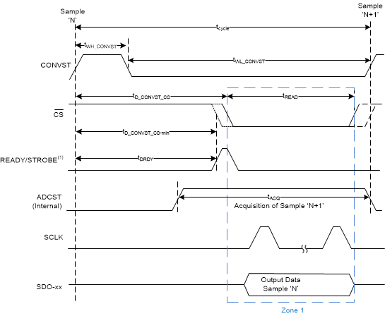
1. The READY output is required for data transfer with zero cycle latency. The STROBE output is required only for clock re-timer (CRT) protocols.
Figure 1. Conversion Control and Data Transfer With Zero Cycle Latency (Zone 1 Transfer) 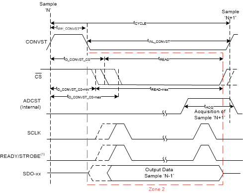
1. The READY output is not required for zone 2 data transfer. The STROBE output is required only for clock re-timer protocols.
Figure 2. Conversion Control and Data Transfer With Wider Read Cycle (Zone 2 Transfer) 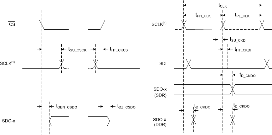
1. The SCLK polarity, launch edge, and capture edge depend on the SPI protocol selected. DDR is not supported with the parallel byte protocol.
Figure 3. SPI-Compatible and Parallel Byte Protocols Timing 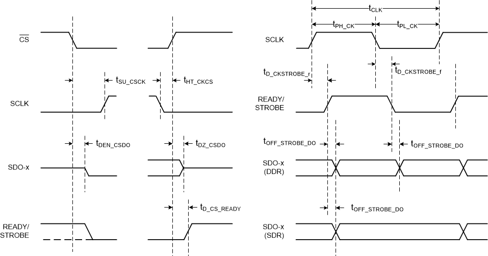 Figure 4. Clock Re-Timer Protocol (External Clock) Timing
 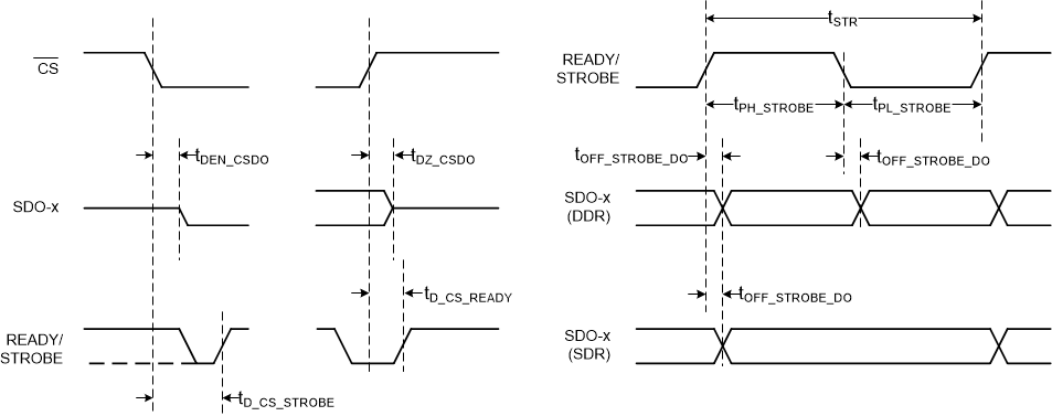 Figure 5. Clock Re-Timer Protocol (Internal Clock) Timing
  Figure 6. Asynchronous Reset and Power-Down Timing