ZHCSIJ5C August 2018 – June 2019 ADS9224R , ADS9234R
PRODUCTION DATA.
- 1 特性
- 2 应用
- 3 说明
- 4 修订历史记录
- 5 Pin Configuration and Functions
-
6 Specifications
- 6.1 Absolute Maximum Ratings
- 6.2 ESD Ratings
- 6.3 Recommended Operating Conditions
- 6.4 Thermal Information
- 6.5 Electrical Characteristics: ADS92x4R
- 6.6 Electrical Characteristics: ADS9224R
- 6.7 Electrical Characteristics: ADS9234R
- 6.8 Timing Requirements
- 6.9 Switching Characteristics
- 6.10 Typical Characteristics: ADS9224R
- 6.11 Typical Characteristics: ADS9234R
-
7 Detailed Description
- 7.1 Overview
- 7.2 Functional Block Diagram
- 7.3 Feature Description
- 7.4 Device Functional Modes
- 7.5 READY/STROBE Output
- 7.6
Programming
- 7.6.1 Output Data Word
- 7.6.2
Data Transfer Protocols
- 7.6.2.1
Protocols for Reading From the Device
- 7.6.2.1.1 Legacy, SPI-Compatible Protocols (SPI-xy-S-SDR)
- 7.6.2.1.2 SPI-Compatible Protocols With Bus Width Options and Single Data Rate (SPI-xy-D-SDR and SPI-xy-Q-SDR)
- 7.6.2.1.3 SPI-Compatible Protocols With Bus Width Options and Double Data Rate (SPI-x1-S-DDR, SPI-x1-D-DDR, SPI-x1-Q-DDR)
- 7.6.2.1.4 Clock Re-Timer (CRT) Protocols (CRT-S-SDR, CRT-D-SDR, CRT-Q-SDR, CRT-S-DDR, CRT-D-DDR, CRT-Q-DDR)
- 7.6.2.1.5 Parallel Byte Protocols (PB-xy-AB-SDR, PB-xy-AA-SDR)
- 7.6.2.2 Device Setup
- 7.6.2.3 Protocols for Configuring the Device
- 7.6.2.1
Protocols for Reading From the Device
- 7.6.3 Reading and Writing Registers
- 7.7
Register Maps
- 7.7.1
ADS92x4R Registers
- 7.7.1.1 DEVICE_STATUS Register (Offset = 0h) [reset = 0h]
- 7.7.1.2 POWER_DOWN_CFG Register (Offset = 1h) [reset = 0h]
- 7.7.1.3 PROTOCOL_CFG Register (Offset = 2h) [reset = 0h]
- 7.7.1.4 BUS_WIDTH Register (Offset = 3h) [reset = 0h]
- 7.7.1.5 CRT_CFG Register (Offset = 4h) [reset = 0h]
- 7.7.1.6 OUTPUT_DATA_WORD_CFG Register (Offset = 5h) [reset = 0h]
- 7.7.1.7 DATA_AVG_CFG Register (Offset = 6h) [reset = 0h]
- 7.7.1.8 REFBY2_OFFSET Register (Offset = 7h) [reset = 0h]
- 7.7.1
ADS92x4R Registers
- 8 Application and Implementation
- 9 Power Supply Recommendations
- 10Layout
- 11器件和文档支持
- 12机械、封装和可订购信息
7.6.2.1.3 SPI-Compatible Protocols With Bus Width Options and Double Data Rate (SPI-x1-S-DDR, SPI-x1-D-DDR, SPI-x1-Q-DDR)
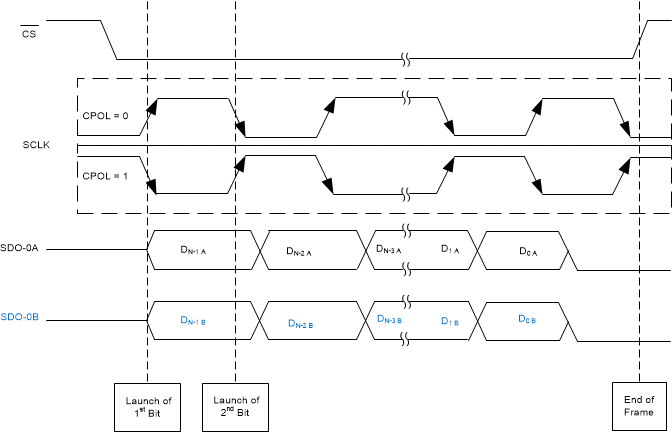
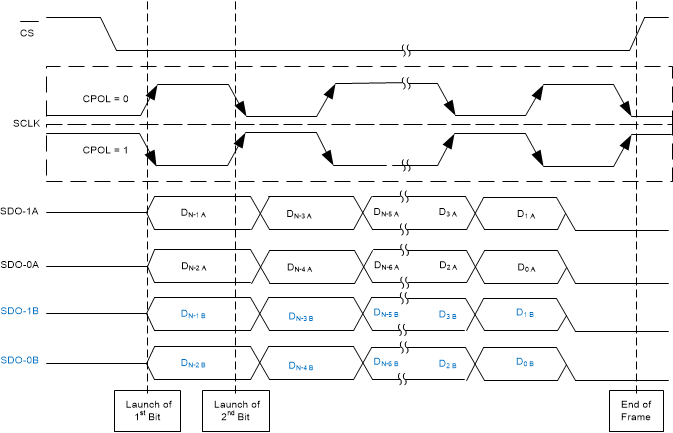
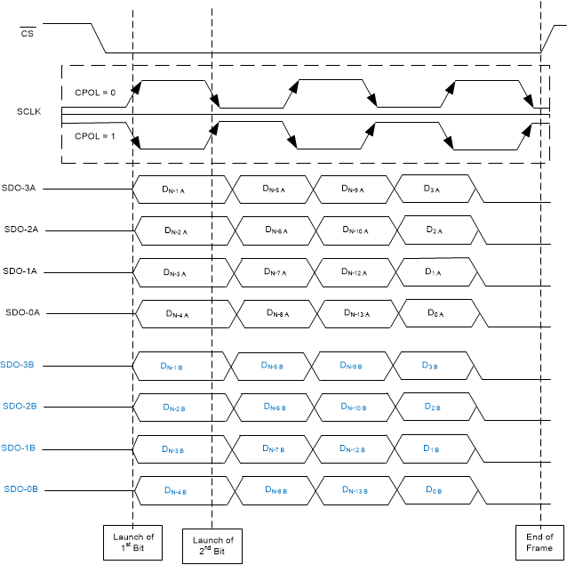
In this data transfer protocol, the data rate for data transfer can be increased to double data rate. With double data rate, the device launches data on both edges (rising and falling) of the SCLK. The device supports both polarities of the clock and only one phase of clock (CPHA = 1). The read time required for reading the output data word reduces with increases in bus width and data rate. The SDOs that are not enabled by the BUS_WIDTH register are set to tri-state. Table 5 provides the details of different SPI protocols with bus width options and double data rate to read data from the device.
Table 5. SPI-x1-S-DDR, SPI-x1-D-DDR, and SPI-x1-Q-DDR Protocols for Reading From Device
| PROTOCOL(1) | SCLK POLARITY (CPOL)(2) | SCLK PHASE(2) | MSB LAUNCH EDGE | BUS WIDTH(5) | tREAD(3)(4) | TIMING DIAGRAM |
|---|---|---|---|---|---|---|
| SPI-01-S-DDR | Low (CPOL = 0) | Falling (CPHA = 1) | 1st SCLK rising | 1 | [9 × tCLK + k] | Figure 53 |
| SPI-11-S-DDR | High (CPOL = 1) | Rising (CPHA = 1) | 1st SCLK falling | 1 | [9 × tCLK + k] | Figure 53 |
| SPI-01-D-DDR | Low (CPOL = 0) | Falling (CPHA = 1) | 1st SCLK rising | 2 | [5 × tCLK + k] | Figure 54 |
| SPI-11-D-DDR | High (CPOL = 1) | Rising (CPHA = 1) | 1st SCLK falling | 2 | [5 × tCLK + k] | Figure 54 |
| SPI-01-Q-DDR | Low (CPOL = 0) | Falling (CPHA = 1) | 1st SCLK rising | 4 | [3 × tCLK + k] | Figure 55 |
| SPI-11-Q-DDR | High (CPOL = 1) | Rising (CPHA = 1) | 1st SCLK falling | 4 | [3 × tCLK + k] | Figure 55 |
Figure 53, Figure 54, and Figure 55 illustrate timing diagrams for the SPI-01-S-DDR and SPI-11-S-DDR, SPI-01-D-DDR and SPI-11-D-DDR, and SPI-01-Q-DDR and SPI-11-Q-DDR protocols, respectively.
 Figure 53. SPI-01-S-DDR and SPI-11-S-DDR Protocols
  Figure 54. SPI-01-D-DDR and SPI-11-D-DDR Protocols
  Figure 55. SPI-01-Q-DDR and SPI-11-Q-DDR Protocols