ZHCS339E August 2010 – June 2019 AFE031
PRODUCTION DATA.
- 1 特性
- 2 应用
- 3 说明
- 4 修订历史记录
- 5 说明(续)
- 6 Device Comparison Table
- 7 Pin Configuration and Functions
-
8 Specifications
- 8.1 Absolute Maximum Ratings
- 8.2 ESD Ratings
- 8.3 Thermal Information
- 8.4 Electrical Characteristics: Transmitter (Tx)
- 8.5 Electrical Characteristics: Power Amplifier (PA)
- 8.6 Electrical Characteristics: Receiver (Rx)
- 8.7 Electrical Characteristics: Digital
- 8.8 Electrical Characteristics: Two-Wire Interface
- 8.9 Electrical Characteristics: Internal Bias Generator
- 8.10 Electrical Characteristics: Power Supply
- 8.11 Timing Requirements
- 8.12 Timing Diagrams
- 8.13 Typical Characteristics
- 9 Detailed Description
- 10Application and Implementation
- 11器件和文档支持
- 12机械、封装和可订购信息
9.2.1 PA Block
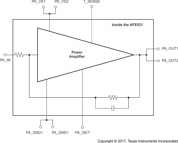
The Power Amplifier (PA) block consists of a high slew rate, high-voltage, and high-current operational amplifier. The PA is configured with an inverting gain of 6.5 V/V, has a low-pass filter response, and maintains excellent linearity and low distortion. The PA is specified to operate from 7 V to 24 V and can deliver up to ±1.5 A of continuous output current over the specified junction temperature range of –40°C to +125°C. Figure 24 illustrates the PA block.
 Figure 24. PA Block Equivalent Circuit
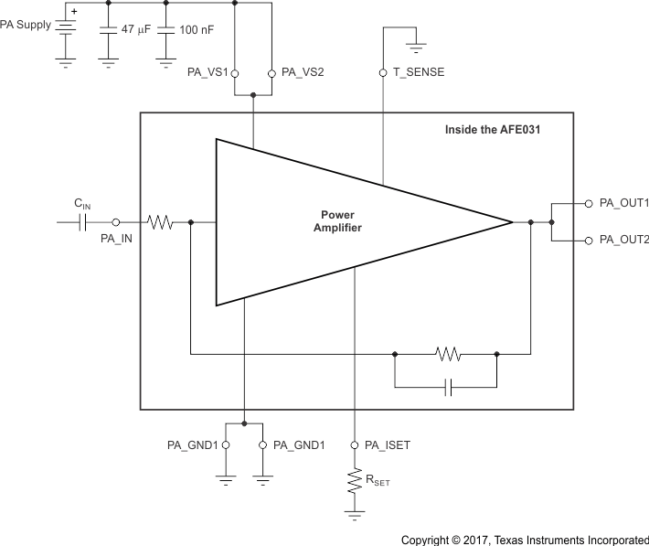
 Connecting the PA in a typical PLC application requires only two additional components: an ac coupling capacitor, CIN, and the current limit programming resistor, RSET. Figure 25 shows the typical connections to the PA block.
 Figure 25. Typical Connections to the PA
 The external capacitor, CIN, introduces a single-pole, high-pass characteristic to the PA transfer function; combined with the inherent low-pass transfer function, this characteristic results in a passband response. The value of the high-pass cutoff frequency is determined by CIN reacting with the input resistance of the PA circuit, and can be found from Equation 1:

Where:
- CIN = external input capacitor
- fHP = desired high-pass cutoff frequency
For example, setting CIN to 3.3 nF results in a high-pass cutoff frequency of 2.4 kHz. The voltage rating for CIN should be determined to withstand operation up to the PA power-supply voltage.
When the transmitter is not in use, the output can be disabled and placed into a high-impedance state by writing a '0' to the PA-OUT bit in the Enable2 Register. Additional power savings can be realized by shutting down the PA when not in use. Shutting down the PA for power savings is accomplished by writing a '0' to the PA bit in the Enable1 Register. Shutting down the PA also results in the PA output entering a high-impedance state. When the PA shuts down, it consumes only 2 mW of power.
The PA_ISET pin (pin 46) provides a resistor-programmable output current limit for the PA block. Equation 2 determines the value of the external RSET resistor attached to this pin.
Where:
- RSET = the value of the external resistor connected between pin 46 and ground.
- ILIM = the value of the desired current limit for the PA.
Note that to ensure proper design margin with respect to manufacturing and temperature variations, a 30% decrease of the value used in Equation 2 for ILIM over the nominal value of ILIM is recommended. See Figure 20, PA Current Limit vs RSET.
