ZHCS339E August 2010 – June 2019 AFE031
PRODUCTION DATA.
- 1 特性
- 2 应用
- 3 说明
- 4 修订历史记录
- 5 说明(续)
- 6 Device Comparison Table
- 7 Pin Configuration and Functions
-
8 Specifications
- 8.1 Absolute Maximum Ratings
- 8.2 ESD Ratings
- 8.3 Thermal Information
- 8.4 Electrical Characteristics: Transmitter (Tx)
- 8.5 Electrical Characteristics: Power Amplifier (PA)
- 8.6 Electrical Characteristics: Receiver (Rx)
- 8.7 Electrical Characteristics: Digital
- 8.8 Electrical Characteristics: Two-Wire Interface
- 8.9 Electrical Characteristics: Internal Bias Generator
- 8.10 Electrical Characteristics: Power Supply
- 8.11 Timing Requirements
- 8.12 Timing Diagrams
- 8.13 Typical Characteristics
- 9 Detailed Description
- 10Application and Implementation
- 11器件和文档支持
- 12机械、封装和可订购信息
9.2.5 REF1 and REF2 Blocks
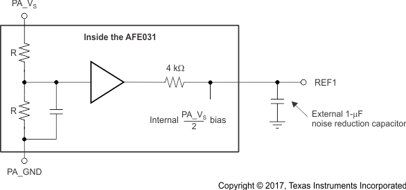
The REF1 and REF2 blocks create midscale power-supply biasing points used internally to the AFE031. Each reference divides its respective power-supply voltage in half with a precision resistive voltage divider. REF1 provides a PA_VS/2 voltage used for the PA, while REF2 provides an AVDD/2 voltage used for the Tx PGA, Tx Filter, Rx PGA1, Rx Filter, and Rx PGA2. Each REF block has its output brought out to an external pin that can be used for filtering and noise reduction. Figure 35 and Figure 36 show the proper connections of the external noise-reducing capacitors. These capacitors are optional, but are recommended for best performance.
 Figure 35. REF1 Functional Diagram
  Figure 36. REF2 Functional Diagram