ZHCSCL7C May   2014  – April 2021 AFE4403

PRODUCTION DATA  

  1. 特性
  2. 应用
  3. 说明
  4. Revision History
  5. Device Family Options
  6. Pin Configuration and Functions
  7. Specifications
    1. 7.1 Absolute Maximum Ratings
    2. 7.2 ESD Ratings
    3. 7.3 Recommended Operating Conditions
    4. 7.4 Thermal Information
    5. 7.5 Electrical Characteristics
    6. 7.6 Timing Requirements
    7. 7.7 Timing Requirements: Supply Ramp and Power-Down
    8. 7.8 Typical Characteristics
  8. Detailed Description
    1. 8.1 Overview
    2. 8.2 Functional Block Diagram
    3. 8.3 Feature Description
      1. 8.3.1 Receiver Channel
        1. 8.3.1.1 Receiver Front-End
        2. 8.3.1.2 Ambient Cancellation Scheme and Second Stage Gain Block
        3. 8.3.1.3 Receiver Control Signals
        4. 8.3.1.4 Receiver Timing
      2. 8.3.2 Clocking and Timing Signal Generation
      3. 8.3.3 Timer Module
        1. 8.3.3.1 Using the Timer Module
      4. 8.3.4 Receiver Subsystem Power Path
      5. 8.3.5 Transmit Section
        1. 8.3.5.1 Third LED Support
        2. 8.3.5.2 Transmitter Power Path
        3. 8.3.5.3 LED Power Reduction During Periods of Inactivity
        4. 8.3.5.4 LED Configurations
    4. 8.4 Device Functional Modes
      1. 8.4.1 ADC Operation and Averaging Module
        1. 8.4.1.1 Operation Without Averaging
        2. 8.4.1.2 Operation With Averaging
        3. 8.4.1.3 Dynamic Power-Down Mode
      2. 8.4.2 Diagnostics
        1. 8.4.2.1 Photodiode-Side Fault Detection
        2. 8.4.2.2 Transmitter-Side Fault Detection
        3. 8.4.2.3 Diagnostics Module
    5. 8.5 Programming
      1. 8.5.1 Serial Programming Interface
      2. 8.5.2 Reading and Writing Data
        1. 8.5.2.1 Writing Data
        2. 8.5.2.2 Reading Data
        3. 8.5.2.3 Multiple Data Reads and Writes
        4. 8.5.2.4 Register Initialization
        5. 8.5.2.5 AFE SPI Interface Design Considerations
    6. 8.6 Register Maps
      1. 8.6.1 AFE Register Map
      2. 8.6.2 AFE Register Description
  9. Application Information Disclaimer
    1. 9.1 Application Information
    2. 9.2 Typical Application
      1. 9.2.1 Design Requirements
      2. 9.2.2 Detailed Design Procedure
      3. 9.2.3 Application Curves
  10. 10Power Supply Recommendations
    1. 10.1 Power Consumption Considerations
  11. 11Layout
    1. 11.1 Layout Guidelines
    2. 11.2 Layout Example
  12. 12Device and Documentation Support
    1. 12.1 Trademarks
    2. 12.2 静电放电警告
    3. 12.3 术语表
  13. 13Mechanical, Packaging, and Orderable Information

封装选项

机械数据 (封装 | 引脚)
散热焊盘机械数据 (封装 | 引脚)
订购信息

LED Power Reduction During Periods of Inactivity

The diagram in Figure 8-20 shows how LED bias current passes 50 µA whenever LED_ON occurs. In order to minimize power consumption in periods of inactivity, the LED_ON control must be turned off. Furthermore, the TIMEREN bit in the CONTROL1 register should be disabled by setting the value to 0.

Note that depending on the LEDs used, the LED may sometimes appear dimly lit even when the LED current is set to 0 mA. This appearance is because of the switching leakage currents (as shown in Figure 8-20) inherent to the timer function. The dimmed appearance does not effect the ambient light level measurement because during the ambient cycle, LED_ON is turned off for the duration of the ambient measurement.
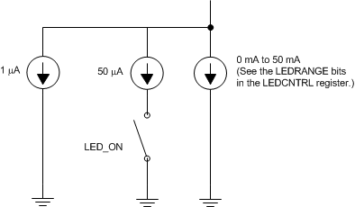
GUID-9244D80A-E011-490B-9312-2DDF6C5EF91F-low.gifFigure 8-20 LED Bias Current