ZHCSCL7C May 2014 – April 2021 AFE4403
PRODUCTION DATA
- 1 特性
- 2 应用
- 3 说明
- 4 Revision History
- 5 Device Family Options
- 6 Pin Configuration and Functions
- 7 Specifications
- 8 Detailed Description
- 9 Application Information Disclaimer
- 10Power Supply Recommendations
- 11Layout
- 12Device and Documentation Support
- 13Mechanical, Packaging, and Orderable Information
9.2.3 Application Curves
This section outlines the trends seen in the Typical Characteristics curves from an application perspective.
Figure 7-5 illustrates the receiver currents in external clock mode with CLKOUT tri-stated. The curve in Figure 7-5 are taken without the dynamic power-down feature enabled, so much lower currents can be achieved using the dynamic power-down feature. Enabling the crystal mode or removing the CLKOUT tri-state increases the receiver currents from the values depicted in the curve.
Figure 7-6 illustrates the transmitter currents with a zero LED current setting. The average LED current can be computed based on the value of the PRF and LED pulse durations, and can be added to the LED_DRV_SUP current described in Figure 7-6.
Figure 7-7 illustrates the total receiver current (analog plus digital supply) for different clock divider ratios. For each clock divider ratio, the external clock frequency is swept in frequency such that the divided clock changes between 3 MHz to 7 MHz. Note however that the supported range for the divided clock is 4 MHz to 6 MHz at each division ratio. Also, the external clock should be limited to be between 4 MHz to 60 MHz.
Figure 7-8 illustrates the power savings arising out of the dynamic power-down mode. This mode can be set by defining the start and end points for the signal PDN_CYCLE within the pulse repetition period. In Figure 7-8, the LED pulse durations are chosen to be 100 µs and the conversions are also chosen to be 100 µs wide. Thus, the entire active period fits in 500 µs. With the timing margins for t1 and t2 indicated in Figure 8-30, the PDN_CYCLE pulse spans the rest of the pulse repetition period. As PRF reduces, the duty cycle of the PDN_CYCLE pulse (as a fraction of the pulse repetition period) increases, which is the reason for the power reduction at lower PRFs as seen in Figure 7-8.
Figure 7-9 illustrates the power savings as a function of the PDN_CYCLE duration at a fixed PRF of 100 Hz. A 100-Hz PRF corresponds to a period of 10 ms. Figure 7-9 indicates the PDN_CYCLE duration swept from 0 ms to 9 ms. With higher durations of PDN_CYCLE, the receiver power reduces.
Figure 7-10 illustrates the baseband response of the switched RC filter for a 5% and 25% duty cycle. When the duty cycle reduces, the effective bandwidth of the filter reduces.
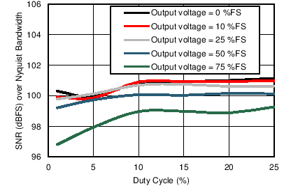
Figure 9-3 shows the SNR of the signal chain as a function of the output voltage level. The data are taken by looping back the transmitter outputs to the receiver inputs using an external op amp that converts the transmitter voltage to a receiver input current. The loopback op amp and external resistors are an extra source of noise in this measurement, so the actual noise levels are higher than the total noise of the transmitter plus the receiver. The SNR in this curve (and other curves) is expressed in terms of dBFS, where the full-scale of the channel is used as the reference level. Because the valid operating range of the signal chain is ±1 V, a full-scale of 2 V is used for converting the output noise to a dBFS number. %FS refers to the percentage of the output level as a function of the positive full-scale. For example, a 50 %FS curve corresponds to the case where the output level is 0.5 V. Also, the total noise in this curve is the total integrated noise in the digital output. All noise is contained in the Nyquist band, which extends from –PRF / 2 to PRF / 2.
 Figure 9-3 SNR over Nyquist Bandwidth vs Duty Cycle (Input Current with Tx-Rx Loopback)
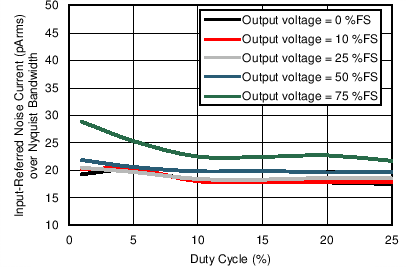
Figure 9-4 is a representation of the same data as Figure 7-10. However, the noise is represented in terms of the input-referred noise current in pArms. By multiplying this number with the TIA gain setting (500 k in this case), the output noise voltage can be computed.
 Figure 9-4 Input-Referred Noise Current over Nyquist Bandwidth vs Duty Cycle (Input Current with Tx-Rx Loopback)
Figure 7-13 illustrates the SNR from the receiver as a function of the sampling duty cycle (which is the sampling pulse duration referred to the pulse repetition period) for different settings of TIA gain. This curve is taken at 100-Hz PRF. The maximum duty cycle is limited to 25%. A lower sampling duty cycle also means a lower LED pulse duration duty cycle, which results in power saving.
Figure 7-14 illustrates the input-referred noise corresponding to Figure 7-13. Figure 7-15 and Figure 7-16 illustrate the SNR and input-referred noise current in a 0.1-Hz to 20-Hz band for the LED-ambient data. By performing a digital ambient subtraction, the low-frequency noise in the signal chain can be significantly attenuated. The noise levels in the bandwidth of interest are lower than the noise over the full Nyquist bandwidth. For a PPG signal, the signal band of interest is usually less than 10 Hz. By performing some digital low-pass filtering in the processor, this noise reduction can be achieved. Figure 7-17 and Figure 7-18 illustrate the noise reduction from ADC averaging. TI therefore recommends setting the number of ADC averages to the maximum allowed at a given PRF. Figure 7-19 and Figure 7-20 illustrate the noise at different PRFs over a 20-Hz bandwidth. At a higher PRF, the 20-Hz noise band is a smaller fraction of the Nyquist band. Thus, noise is lower at higher PRFs in these figures. Figure 7-21 and Figure 7-22 illustrate the noise at different PRFs over a 20-Hz bandwidth with dynamic power-down mode enabled. The active window remains as 500 µs and all samples and conversions are performed at this time. For the rest of the period, the device is in dynamic power-down with the t1 and t2 values as described in Figure 8-30. Again, the noise reduces with higher PRF. Figure 7-23 and Figure 7-24 illustrate the noise as a function of the PDN_CYCLE duration varied from 0 ms to 9 ms, with the active duration (available for conversion) occupying the rest of the period. With higher PDN_CYCLE durations, the number of allowed ADC averages reduces, ehich explains the slight increase in noise at higher PDN_CYCLE durations. Figure 7-25 and Figure 7-26 illustrate the noise as a function of temperature over a 20-Hz bandwidth. The measurements are performed with a transmit-receive loopback as explained earlier. The input current is maintained at 1 µA. Thus, for 250-k gain setting, the output voltage is 0.5 V and for a 500-k gain setting, the output voltage is 1 V. Figure 7-27 and Figure 7-28 illustrate the noise reduction using additional gain in stage 2. Figure 7-29 shows the noise as a function of the internal (divided) clock frequency. The external clock is varied from 7 MHz to 14 MHz with a clock division ratio of 2. This range of external clock results in the internal clock varying from 3.5 MHz to 7 MHz. Out of this range, 4 MHz to 6 MHz is the allowed range for the internal (divided) clock at all clock division ratios. Figure 7-30 illustrates the deviation in the measured LED current with respect to the calculated current when the LED current code is swept from 0 to 255 in steps of 1.
Figure 7-31 and Figure 7-32 illustrate the transmitter+receiver noise (in external loopback mode) as a function of the TX_REF voltage setting. At lower TX_REF voltages, there is a slight increase in the transmitter noise. This increase is not very apparent from the curves because the transmitter noise is at a level much lower than the total noise. Figure 7-33 illustrates the transmitter current as a function of the current setting code. Figure 7-34 illustrates the spread of the transmitter current taken across a large number of devices for the same current setting. Figure 7-35 illustrates how the LED current changes linearly with the TX_REF voltage for a fixed code.