ZHCSCL7C May 2014 – April 2021 AFE4403
PRODUCTION DATA
- 1 特性
- 2 应用
- 3 说明
- 4 Revision History
- 5 Device Family Options
- 6 Pin Configuration and Functions
- 7 Specifications
- 8 Detailed Description
- 9 Application Information Disclaimer
- 10Power Supply Recommendations
- 11Layout
- 12Device and Documentation Support
- 13Mechanical, Packaging, and Orderable Information
8.3.5 Transmit Section
The transmit section integrates the LED driver and the LED current control section with 8-bit resolution.
The RED and IR LED reference currents can be independently set. The current source (ILED) locally regulates and ensures that the actual LED current tracks the specified reference. The transmitter section uses an internal 0.25-V reference voltage for operation. This reference voltage is available on the TX_REF pin and must be decoupled to ground with a 2.2-μF capacitor. The TX_REF voltage is derived from the TX_CTRL_SUP. The TX_REF voltage can be programmed from 0.25 V to 1 V. A lower TX_REF voltage allows a lower voltage to be supported on LED_DRV_SUP. However, the transmitter dynamic range falls in proportion to the voltage on TX_REF. Thus, a TX_REF setting of 0.5 V gives a 6-dB lower transmitter dynamic range as compared to a 1-V setting on TX_REF, and a 6-dB higher transmitter dynamic range as compared to a 0.25-V setting on TX_REF.
Note that reducing the value of the band-gap reference capacitor on the BG pin reduces the time required for the device to wake-up and settle. However, this reduction in time is a trade-off between wake-up time and noise performance.For example, reducing the value of the capacitors on the BG and TX_REF pins from 2.2 uF to 0.1 uF reduces the wake-up time (from complete power-down) from 1000 ms to 100 ms, but results in a few decibels of degradation in the transmitter dynamic range.
The minimum LED_DRV_SUP voltage required for operation depends on:
- Voltage drop across the LED (VLED),
- Voltage drop across the external cable, connector, and any other component in series with the LED (VCABLE), and
- Transmitter reference voltage.
See the Recommended Operating Conditions table for further details.
Two LED driver schemes are supported:
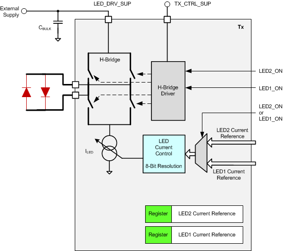
- An H-bridge drive for a two-terminal back-to-back LED package; see Figure 8-16.
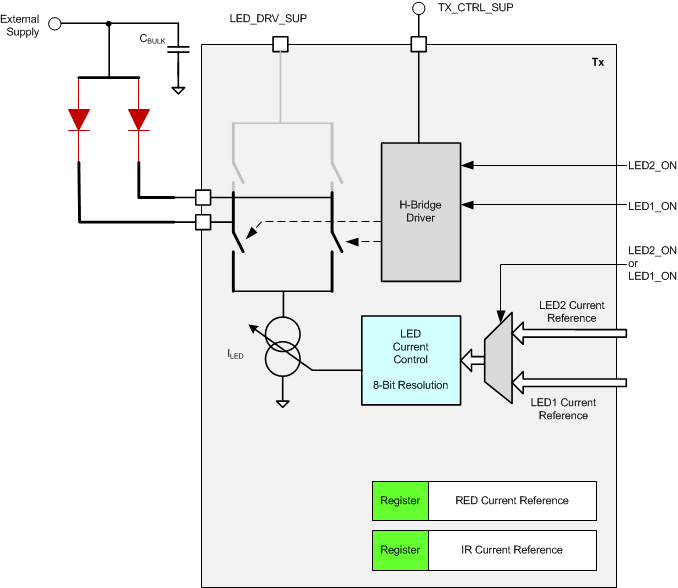
- A push-pull drive for a three-terminal LED package; see Figure 8-17.
 Figure 8-16 Transmit: H-Bridge Drive
 Figure 8-17 Transmit: Push-Pull LED Drive for Common Anode LED Configuration