At PRF = 100 Hz, 25% duty cycle, RF = 500 kΩ, CF is adjusted to keep TIA time constant at 1/10th of sampling duration, All supplies at 3.3 V, 8-MHz external clock, CLKOUT tri-state, 1-µF capacitor on TX_REF and BG pins, detector CIN = 50 pF, TX_REF = 0.5 V, ADC averaging = max allowed, and SNR in dBFS is noise referred to full-scale range of 2 V, unless otherwise noted.
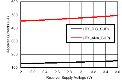 Figure 7-5 Receiver Currents vs Receiver Supply Voltage
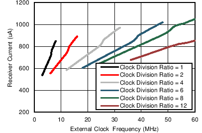 Figure 7-7 Receiver Currents (Analog and Digital) vs Clock Divider Ratio
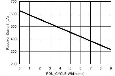
| PRF = 100 Hz |
LED pulse = 100 µs |
| All
four DYNAMIC bits set to 1 |
Figure 7-9 Receiver Current (Analog and Digital) vs Dynamic Power-Down Duty
Cycle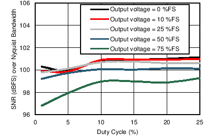 Figure 7-11 SNR
over Nyquist Bandwidth vs Duty Cycle (Input Current with Tx-Rx
Loopback)
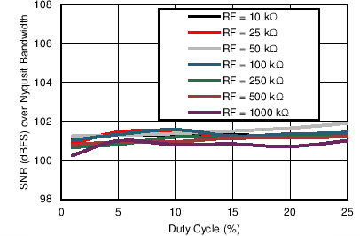 Figure 7-13 Receiver SNR over Nyquist Bandwidth vs Duty Cycle (Different Gain
Settings)
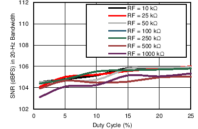 Figure 7-15 Receiver SNR in 20-Hz BW vs Duty Cycle (Different Gain Settings)
 Figure 7-17 Receiver SNR over Nyquist Bandwidth vs Duty Cycle (Different ADC
Averaging)
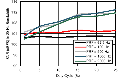 Figure 7-19 Receiver SNR in 20-Hz BW vs Duty Cycle (Different PRFs)
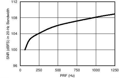
| Active window = 500
µs |
LED pulse = 100 µs |
| All
four DYNAMIC bits set to 1 |
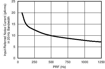
Figure 7-21 Receiver SNR in 20-Hz BW in Dynamic Power-Down Mode vs PRF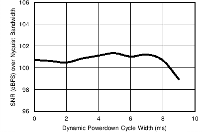
| PRF = 100 Hz |
LED pulse = 100 µs |
| All
four DYNAMIC bits set to 1 |
Figure 7-23 Receiver SNR over Nyquist Bandwidth vs Dynamic Power-Down Duty
Cycle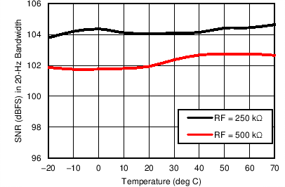
| LED
pulse = 100 µs |
Pleth current =
1 µA |
Figure 7-25 SNR
in 20-Hz Bandwidth vs Temperature (Tx-Rx Loopback)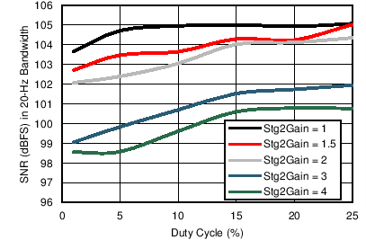 Figure 7-27 Receiver SNR over Nyquist Bandwidth vs Duty Cycle (Different Stage 2 Gain
Settings)
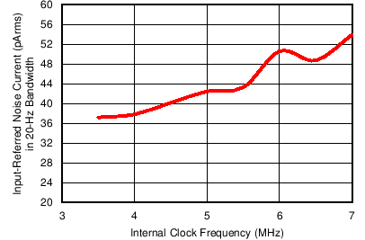
| RF = 250
kΩ |
PRF = 100 Hz |
ADC averaging = 1 |
Figure 7-29 Receiver Input-Referred Noise Current vs Internal Clock Frequency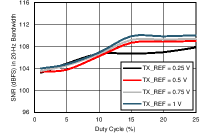
| PRF = 500 Hz |
|
|
| DAC
current is set such that ADC output is 50 %FS |
Figure 7-31 SNR
in 20-Hz BW vs Duty Cycle (TX_REF Voltage with Tx-Rx Loopback)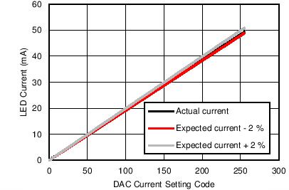 Figure 7-33 Transmitter Current linearity
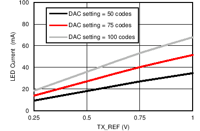 Figure 7-35 Transmitter Current vs TX_REF Voltage (Multiple DAC Settings)
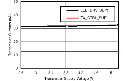 Figure 7-6 Transmitter Currents vs Transmitter Supply Voltage
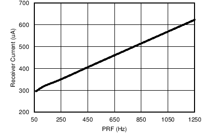
| Active window = 500
µs |
LED pulse = 100 µs |
| All
four DYNAMIC bits set to 1 |
Figure 7-8 Receiver Current vs PRF in Dynamic Power-Down Mode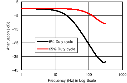 Figure 7-10 Filter Response vs Duty cycle
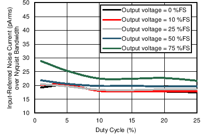 Figure 7-12 Input-Referred Noise Current over Nyquist Bandwidth vs Duty Cycle (Input
Current with Tx-Rx Loopback)
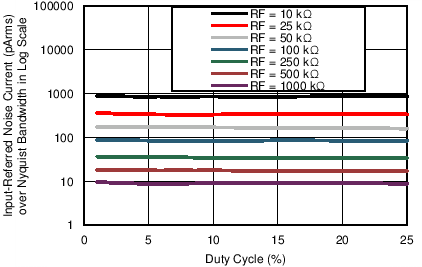 Figure 7-14 Receiver Input-Referred Noise Current over Nyquist Bandwidth vs Duty Cycle
(Different Gain Settings)
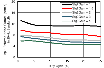
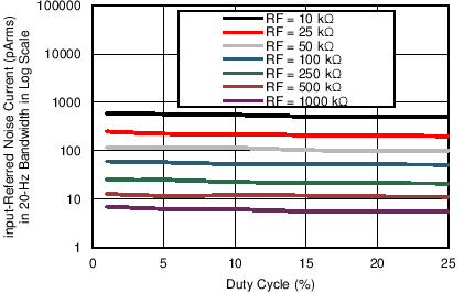 Figure 7-16 Receiver Input-Referred Noise Current in 20-Hz BW vs Duty Cycle (Different
Gain Settings)
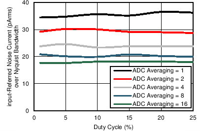 Figure 7-18 Receiver Input-Referred Noise Current over Nyquist Bandwidth vs Duty Cycle
(Different ADC Averaging)
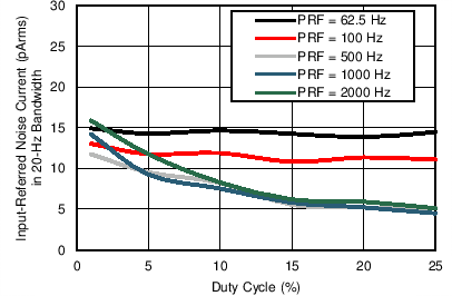 Figure 7-20 Receiver Input Referred Noise in 20-Hz BW vs Duty Cycle (Different
PRFs)
| Active window = 500
µs |
LED pulse = 100 µs |
| All
four DYNAMIC bits set to 1 |
Figure 7-22 Receiver Input-Referred Noise in 20-Hz BW in Dynamic Power-Down Mode vs
PRF
| PRF = 100 Hz |
LED pulse = 100 µs |
| All
four DYNAMIC bits set to 1 |
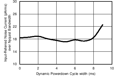
Figure 7-24 Receiver Input-Referred Noise over Nyquist Bandwidth vs Dynamic Power-Down
Duty Cycle
| LED
pulse = 100 µs |
Pleth current =
1 µA |
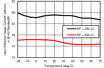
Figure 7-26 Input-Referred Noise Current in 20-Hz BW vs Temperature (TX-Rx
Loopback) Figure 7-28 Receiver Input-Referred Noise Current over Nyquist Bandwidth vs Duty Cycle
(Different Stage 2 Gain Settings)
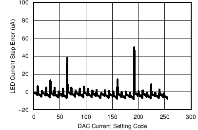
 Figure 7-30 Transmitter DAC Current Step Error
| PRF = 500 Hz |
|
|
| DAC
current is set such that ADC output is 50 %FS |
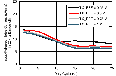
Figure 7-32 Input
Referred Noise Current in 20-Hz BW vs Duty Cycle (TX_REF Voltage with Tx-Rx
Loopback)
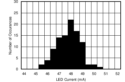
| LED current = 48
mA |
100 devices on
tester |
Figure 7-34 Transmitter Current Across Devices Figure 7-5 Receiver Currents vs Receiver Supply Voltage


 Figure 7-13 Receiver SNR over Nyquist Bandwidth vs Duty Cycle (Different Gain
Settings)
 Figure 7-15 Receiver SNR in 20-Hz BW vs Duty Cycle (Different Gain Settings)
 Figure 7-17 Receiver SNR over Nyquist Bandwidth vs Duty Cycle (Different ADC
Averaging)
 Figure 7-19 Receiver SNR in 20-Hz BW vs Duty Cycle (Different PRFs)


 Figure 7-35 Transmitter Current vs TX_REF Voltage (Multiple DAC Settings)


 Figure 7-14 Receiver Input-Referred Noise Current over Nyquist Bandwidth vs Duty Cycle
(Different Gain Settings)
 Figure 7-16 Receiver Input-Referred Noise Current in 20-Hz BW vs Duty Cycle (Different
Gain Settings)
 Figure 7-18 Receiver Input-Referred Noise Current over Nyquist Bandwidth vs Duty Cycle
(Different ADC Averaging)
 Figure 7-20 Receiver Input Referred Noise in 20-Hz BW vs Duty Cycle (Different
PRFs)