ZHCSP80 December 2022 AFE78101 , AFE88101
PRODUCTION DATA
- 1 特性
- 2 应用
- 3 说明
- 4 Revision History
- 5 Pin Configuration and Functions
-
6 Specifications
- 6.1 Absolute Maximum Ratings
- 6.2 ESD Ratings
- 6.3 Recommended Operating Conditions
- 6.4 Thermal Information
- 6.5 Electrical Characteristics
- 6.6 Timing Requirements
- 6.7 Timing Diagrams
- 6.8 Typical Characteristics: VOUT DAC
- 6.9 Typical Characteristics: ADC
- 6.10 Typical Characteristics: Reference
- 6.11 Typical Characteristics: Power Supply
-
7 Detailed Description
- 7.1 Overview
- 7.2 Functional Block Diagram
- 7.3 Feature Description
- 7.4 Device Functional Modes
- 7.5 Programming
- 7.6 Register Maps
- 8 Application and Implementation
- 9 Device and Documentation Support
- 10Mechanical, Packaging, and Orderable Information
7.3.2.5 External Monitoring Inputs
The AFEx8101 have two analog inputs for external voltage sensing. Channels 1 and 2 for the CCS pointer are for external monitoring inputs that can be measured by pins AIN0 and AIN1, respectively. The input range for the analog inputs is configurable to either 0 V to 1.25 V or 0 V to 2.5 V. The analog inputs conversion values are stored in straight binary format in the ADC registers. The ADC resolution can be computed by Equation 7:
where
- VRANGE = 2.5 V for the 0‑V to 2.5‑V input range or 1.25 V for the 0‑V to 1.25‑V input range.
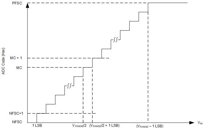
Figure 7-10 and Table 7-6 detail the transfer characteristics.
 Figure 7-10 ADC Transfer
Characteristics
Figure 7-10 ADC Transfer
Characteristics| INPUT VOLTAGE | CODE | DESCRIPTION | IDEAL OUTPUT CODE |
|---|---|---|---|
| ≤1 LSB | NFSC | Negative full-scale code | 000 |
| 1 LSB to 2 LSB | NFSC + 1 | Negative full-scale code plus 1 | 001 |
| (VRANGE / 2) to (VRANGE / 2) + 1 LSB | MC | Midcode | 800 |
| (VRANGE / 2) + 1 LSB to (VRANGE / 2) + 2 LSB | MC + 1 | Midcode plus 1 | 801 |
| ≥ VRANGE – 1 LSB | PFSC | Positive full-scale code | FFF |
For these external monitoring inputs, the ADC is configurable for both data rate and voltage range. The data rate is set to either 640 Hz, 1280 Hz, 2560 Hz, or 3840 Hz with the ADC_CFG.CONV_RATE bits. The range of the ADC measurement is set with the ADC_CFG.AIN_RANGE bit. The ADC range is 2 × VREF when the bit = 0; the ADC range is VREF when the bit = 1. ADC_CFG.AIN_RANGE only controls the range if PVDD > 2.7 V. When PVDD = 1.8 V, the range is VREF regardless of the setting.
When the ADC conversion is completed for AIN0 and AIN1, the resulting ADC data are stored in the ADC_AIN0.DATA and ADC_AIN1.DATA bits at 24h and 25h of the register map.
If the external monitoring inputs are not used, connect the AIN0 and AIN1 pins to GND through a 1-kΩ resistor.