ZHCSP80 December 2022 AFE78101 , AFE88101
PRODUCTION DATA
- 1 特性
- 2 应用
- 3 说明
- 4 Revision History
- 5 Pin Configuration and Functions
-
6 Specifications
- 6.1 Absolute Maximum Ratings
- 6.2 ESD Ratings
- 6.3 Recommended Operating Conditions
- 6.4 Thermal Information
- 6.5 Electrical Characteristics
- 6.6 Timing Requirements
- 6.7 Timing Diagrams
- 6.8 Typical Characteristics: VOUT DAC
- 6.9 Typical Characteristics: ADC
- 6.10 Typical Characteristics: Reference
- 6.11 Typical Characteristics: Power Supply
-
7 Detailed Description
- 7.1 Overview
- 7.2 Functional Block Diagram
- 7.3 Feature Description
- 7.4 Device Functional Modes
- 7.5 Programming
- 7.6 Register Maps
- 8 Application and Implementation
- 9 Device and Documentation Support
- 10Mechanical, Packaging, and Orderable Information
7.3.1.5 Programmable Slew Rate
The slew rate feature controls the rate at which the output voltage or current changes. This feature is disabled by default and is enabled by writing a logic 1 to the DAC_CFG.SR_EN bit. With the slew rate control feature disabled, the output changes smoothly at a rate limited by the output drive circuitry and the attached load.
With this feature enabled, the output does not slew directly between the two values. Instead, the output steps digitally at a rate defined by DAC_CFG.SR_STEP[2:0] and DAC_CFG.SR_CLK[2:0]. SR_CLK defines the rate at which the digital slew updates. SR_STEP defines the amount by which the output value changes at each update. Section 7.6.1 shows different settings for SR_STEP and SR_CLK.
The time required for the output to slew is expressed as Equation 6:
where
- Slew Time is expressed in seconds
- Slew Step is controlled by DAC_CFG.SR_STEP
- Slew Clock Rate is controlled by DAC_CFG.SR_CLK
When the slew-rate control feature is enabled, the output changes at the programmed slew rate. This configuration results in a staircase formation at the output. If the clear code is asserted (see Section 7.3.1.6), the output slews to the DAC_CLR_CODE value at the programmed slew rate. When new DAC data are written, the output starts slewing to the new value at the slew rate determined by the current DAC code and the new DAC data. The update clock frequency for any given value is the same for all output ranges. The step size, however, varies across output ranges for a given value of step size because the LSB size is different for each output range.
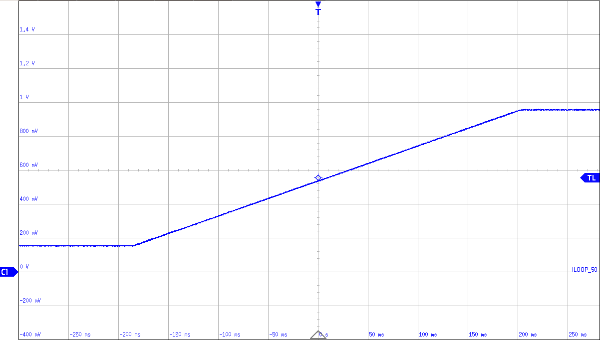
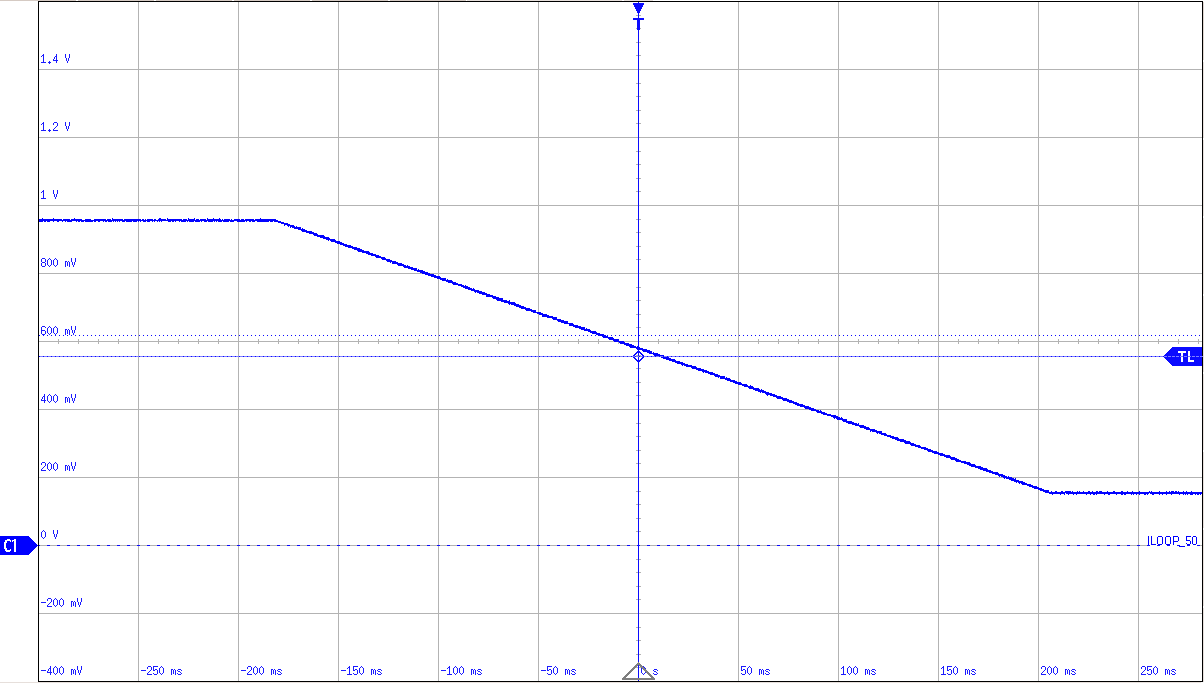
Two slew-rate control modes are available: linear (default) and sinusoidal. Figure 7-3 and Figure 7-4 show the typical rising and falling DAC output waveforms, respectively.

| 4 mA (0x0BA3) to 24 mA (0xF45D) measured on a 40-Ω shunt |

| 24 mA (0xF45D) to 4 mA (0x0BA3) measured on 40-Ω shunt |
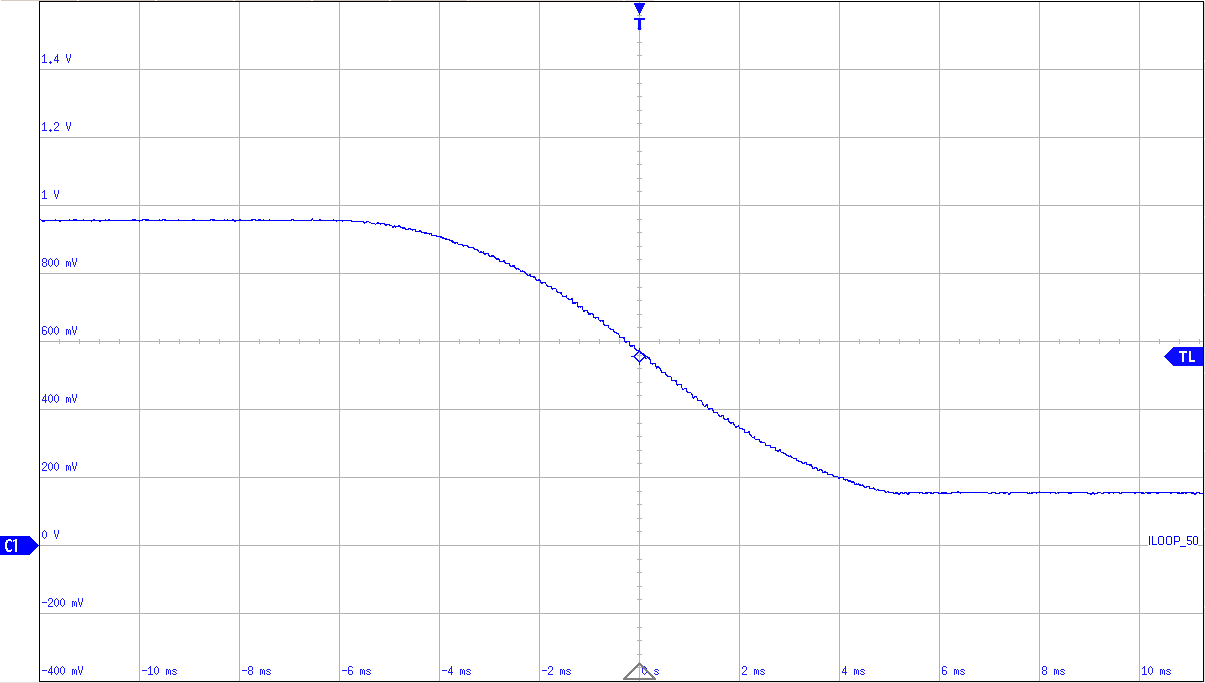
Sinusoidal mode enables fast DAC settling while improving analog rate of change characteristics. Sinusoidal mode is selected by the DAC_CFG.SR_MODE bit. Figure 7-5 and Figure 7-6 show the typical rising and falling DAC output waveforms with sinusoidal slew-rate control, respectively.

| 4 mA (0x0BA3) to 24 mA (0xF45D) measured on a 40-Ω shunt |

| 24 mA (0xF45D) to 4 mA (0x0BA3) measured on a 40-Ω shunt |
If the slew-rate feature is disabled while the DAC is executing the slew-rate command, the slew-rate operation is aborted, and the DAC output goes to the target code.