Typical values at TA =
+25°C with nominal supplies. Unless otherwise noted, TX input data rate = 500 MSPS,
fDAC = 9000 MSPS, non-interleave mode, AOUT = –1
dBFS, 2nd Nyquist zone output, External clock mode, 18x Interpolation,
DSA = 0 dB, Sin(x)/x enabled, DSA calibrated, 7.1 GHz matching.

| Excluding PCB and cable losses |
Figure 6-544 TX
Full Scale vs RF Frequency and Channel
| Excluding PCB and cable losses |
Figure 6-546 TX
Full Scale vs DSA Setting and Channel at 7.1 GHz
| Differential Gain Error = Gain(DSA Setting – 1) –
Gain(DSA Setting) |
Figure 6-548 Uncalibrated Differential Gain Error vs Temperature at 7.1 GHz
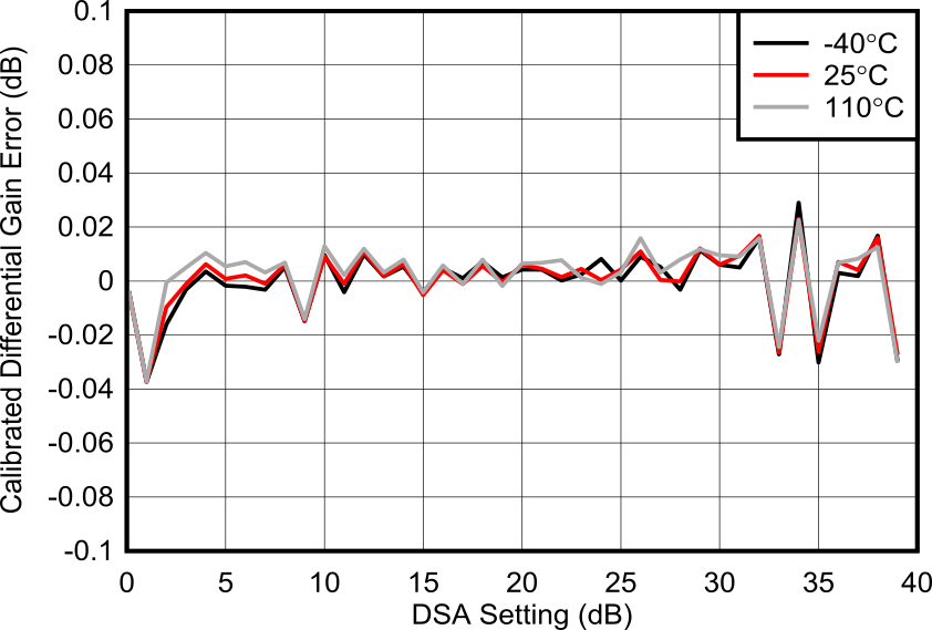
| Differential Gain Error = Gain(DSA Setting – 1) –
Gain(DSA Setting) |
Figure 6-550 Calibrated Differential Gain Error vs Temperature at 7.1 GHz
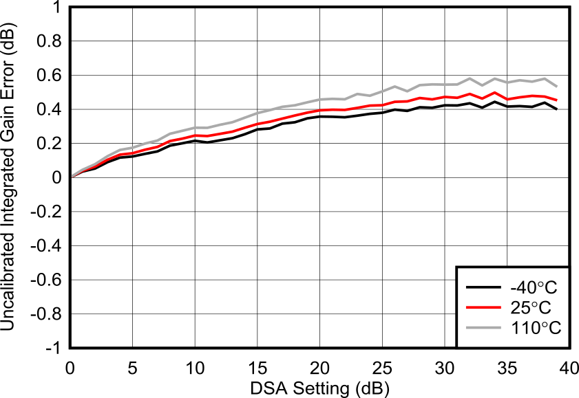
| Integrated Gain Error = Gain(DSA Setting) – Gain(DSA
Setting = 0). |
Figure 6-552 Uncalibrated Integrated Gain Error vs Temperature at 7.1 GHz
| Integrated Gain Error = Gain(DSA Setting) – Gain(DSA
Setting = 0). |
Figure 6-554 Calibrated Integrated Gain Error vs Temperature at 7.1 GHz
| Differential Phase Error = Phase(DSA Setting – 1) –
Phase(DSA Setting) |
Figure 6-556 Uncalibrated Differential Phase Error vs Temperature at 7.1 GHz
| Differential Phase Error = Phase(DSA Setting – 1) –
Phase(DSA Setting) |
Figure 6-558 Calibrated Differential Phase Error vs Temperature at 7.1 GHz
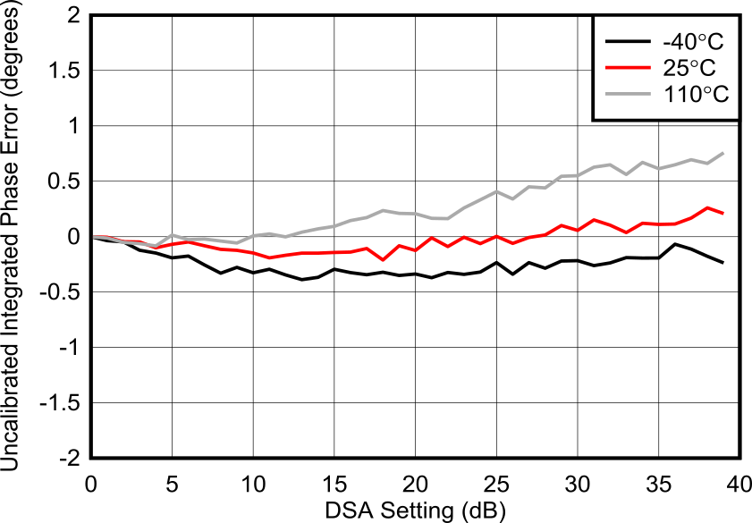
| Integrated Phase Error = Phase(DSA Setting) – Phase(DSA
Setting = 0) |
Figure 6-560 Uncalibrated Integrated Phase Error vs Temperature at 7.1 GHz
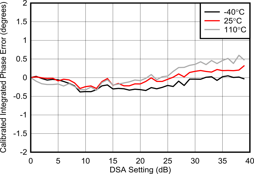
| Integrated Phase Error = Phase(DSA Setting) – Phase(DSA
Setting = 0) |
Figure 6-562 Calibrated Integrated Phase Error vs Temperature at 7.1 GHz Figure 6-564 IMD3 vs Digital Amplitude and Temperature at 7.1
GHz
 Figure 6-566 IMD3 vs DSA Setting and Digital Amplitude at 7.1
GHz
 Figure 6-568 IMD3
vs Tone Spacing and Channel at 7.1 GHz
 Figure 6-570 IMD3 vs Tone Spacing and Temperature at 7.1
GHz
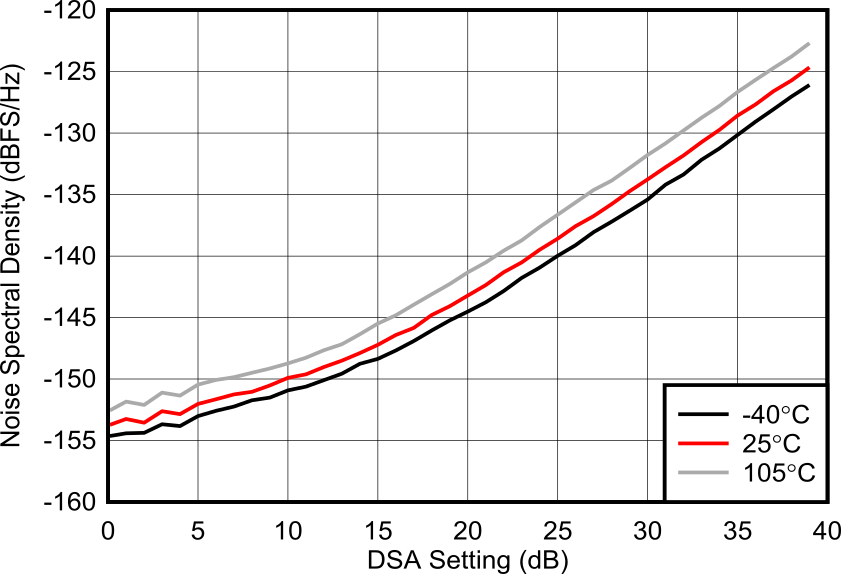
 Figure 6-572 NSD
vs DSA Setting and Amplitude at 7.1 GHz
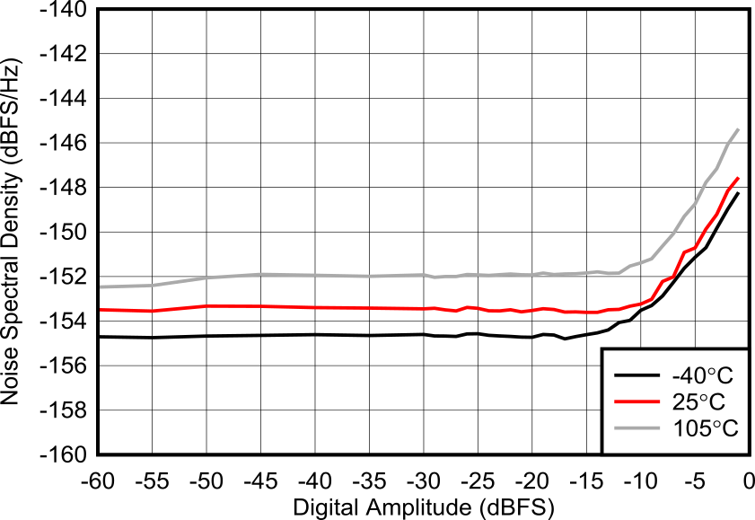
 Figure 6-574 NSD
vs Digital Amplitude and Channel at 7.1 GHz
| 50 MHz
tone spacing, inband = 7100 MHz ± 200 MHz, excluding
IMD3 components separately |
Figure 6-576 Two
Tone Inband SFDR vs Output Amplitude at 7.1 GHz Figure 6-578 Single Tone Output Spectrum at 7.1 GHz, -1 dBFS (narrow span)
 Figure 6-580 Single Tone Output Spectrum at 7.1 GHz, -6 dBFS (narrow span)
 Figure 6-582 Single Tone Output Spectrum at 7.1 GHz, -12 dBFS (narrow span)
 Figure 6-584 Two
Tone Output Spectrum at 7.1 GHz, -7 dBFS each (narrow band)
 Figure 6-586 Two
Tone Output Spectrum at 7.1 GHz, -13 dBFS each (narrow span)
 Figure 6-588 Two
Tone Output Spectrum at 7.1 GHz, -30 dBFS each (narrow span)
| Excluding PCB and cable losses |
Figure 6-545 TX
Full Scale vs Temperature and Channel at 7.1 GHz
| Differential Gain Error = Gain(DSA Setting – 1) –
Gain(DSA Setting) |
Figure 6-547 Uncalibrated Differential Gain Error vs Channel at 7.1 GHz
| Differential Gain Error = Gain(DSA Setting – 1) –
Gain(DSA Setting) |
Figure 6-549 Calibrated Differential Gain Error vs Channel at 7.1 GHz
| Integrated Gain Error = Gain(DSA Setting) – Gain(DSA
Setting = 0). |
Figure 6-551 Uncalibrated Integrated Gain Error vs Channel at 7.1 GHz
| Integrated Gain Error = Gain(DSA Setting) – Gain(DSA
Setting = 0). |
Figure 6-553 Calibrated Integrated Gain Error vs Channel at 7.1 GHz
| Differential Phase Error = Phase(DSA Setting – 1) –
Phase(DSA Setting) |
Figure 6-555 Uncalibrated Differential Phase Error vs Channel at 7.1 GHz
| Differential Phase Error = Phase(DSA Setting – 1) –
Phase(DSA Setting) |
Figure 6-557 Calibrated Differential Phase Error vs Channel at 7.1 GHz
| Integrated Phase Error = Phase(DSA Setting) – Phase(DSA
Setting = 0) |
Figure 6-559 Uncalibrated Integrated Phase Error vs Channel at 7.1 GHz
| Integrated Phase Error = Phase(DSA Setting) – Phase(DSA
Setting = 0) |
Figure 6-561 Calibrated Integrated Phase Error vs Channel at 7.1 GHz Figure 6-563 IMD3
vs Digital Amplitude and Channel at 7.1 GHz
 Figure 6-565 IMD3
vs DSA Setting and Channel at 7.1 GHz
 Figure 6-567 IMD3 vs DSA Setting and Temperature at 7.1
GHz
 Figure 6-569 IMD3 vs Tone Spacing and Digital Amplitude at 7.1
GHz
| Tone
at -12 dBFS, 50 MHz offset from tone |
Figure 6-571 NSD
vs DSA Setting and Channel at 7.1 GHz
| Tone
at -12 dBFS, 50 MHz offset from tone |
Figure 6-573 NSD
vs DSA Setting and Temperature at 7.1 GHz Figure 6-575 NSD
vs Digital Amplitude and Temperature at 7.1 GHz
 Figure 6-577 Single Tone Output Spectrum at 7.1 GHz, -1 dBFS (Nyquist)
 Figure 6-579 Single Tone Output Spectrum at 7.1 GHz, -6 dBFS (Nyquist)
 Figure 6-581 Single Tone Output Spectrum at 7.1 GHz, -12 dBFS (Nyquist)
 Figure 6-583 Two
Tone Output Spectrum at 7.1 GHz, -7 dBFS each (Nyquist)
 Figure 6-585 Two
Tone Output Spectrum at 7.1 GHz, -13 dBFS each (Nyquist)
 Figure 6-587 Two
Tone Output Spectrum at 7.1G Hz, -30 dBFS each (Nyquist)
 Figure 6-589 External Clock Additive Phase Noise at 7.1 GHz


