ZHCSVF3P December 1990 – March 2024 AM26C31
PRODUCTION DATA
- 1
- 1 特性
- 2 应用
- 3 说明
- 4 Pin Configuration and Functions
-
5 Specifications
- 5.1 Absolute Maximum Ratings
- 5.2 ESD Ratings
- 5.3 Recommended Operating Conditions
- 5.4 Thermal Information
- 5.5 Electrical Characteristics: AM26C31C and AM26C31I
- 5.6 Electrical Characteristics: AM26C31Q and AM26C31M
- 5.7 Switching Characteristics: AM26C31C and AM26C31I
- 5.8 Switching Characteristics: AM26C31Q and AM26C31M
- 5.9 Typical Characteristics
- 6 Parameter Measurement Information
- 7 Detailed Description
- 8 Application Information Disclaimer
- 9 Device and Documentation Support
- 10Revision History
- 11Mechanical, Packaging, and Orderable Information
封装选项
机械数据 (封装 | 引脚)
散热焊盘机械数据 (封装 | 引脚)
订购信息
6 Parameter Measurement Information
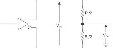
 Figure 6-1 Differential and Common-Mode Output Voltages
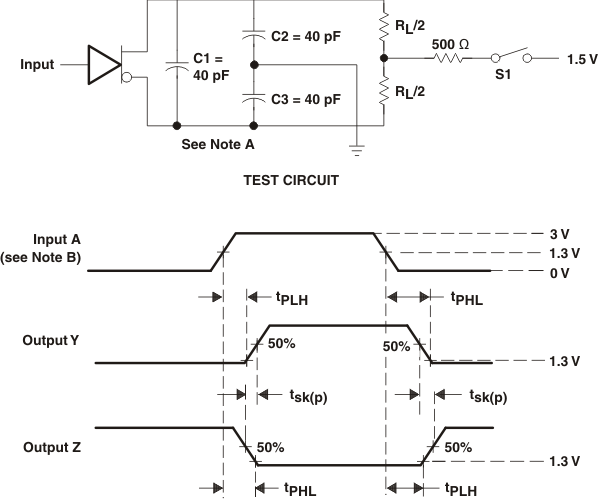
A. C1, C2, and C3 include probe and jig capacitance.
B. All input pulses are supplied by generators having the following characteristics: PRR ≤ 1MHz, duty cycle ≤ 50%, and tr, tf ≤ 6ns.
Figure 6-2 Propagation Delay Time and Skew Waveforms and Test Circuit
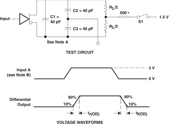
A. C1, C2, and C3 include probe and jig capacitance.
B. All input pulses are supplied by generators having the following characteristics: PRR ≤ 1MHz, duty cycle ≤ 50%, and tr, tf ≤ 6ns.
Figure 6-3 Differential-Output Rise and Fall-Time Waveforms and Test Circuit
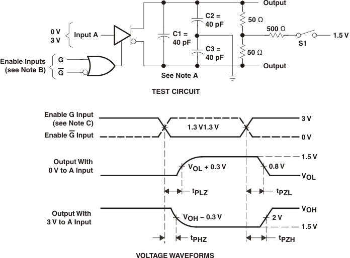
A. C1, C2, and C3 include
probe and jig capacitance.
B. All input pulses are
supplied by generators having the following characteristics: PRR ≤ 1MHz,
duty cycle ≤ 50%, and tr, tf ≤ 6ns.
C. Each enable is tested
separately.
Figure 6-4 Output Enable and Disable Time Waveforms and Test Circuit