ZHCSPJ8B December 2021 – December 2023 AM2732 , AM2732-Q1
PRODUCTION DATA
- 1
- 1 特性
- 2 应用
- 3 说明
- 4 Device Comparison
-
5 Terminal Configuration and Functions
- 5.1 Pin Diagram
- 5.2 Pin Attributes (AM273x ZCE, NZN Packages)
- 5.3
Signal Descriptions
- 5.3.1 ADC Signal Descriptions
- 5.3.2 CPTS Signal Descriptions
- 5.3.3 CSI 2.0 Signal Descriptions
- 5.3.4 DMM Signal Descriptions
- 5.3.5 ECAP Signal Descriptions
- 5.3.6 EPWM Signal Descriptions
- 5.3.7 GPIO Signal Descriptions
- 5.3.8 I2C Signal Descriptions
- 5.3.9 Clock Signal Descriptions
- 5.3.10 JTAG Signal Descriptions
- 5.3.11 LVDS Signal Descriptions
- 5.3.12 MCAN Signal Descriptions
- 5.3.13 MCASP Signal Descriptions
- 5.3.14 Ethernet Signal Descriptions
- 5.3.15 GPIO Signal Descriptions
- 5.3.16 Power Supply Signal Descriptions
- 5.3.17 QSPI Signal Descriptions
- 5.3.18 Reserverd Signal Descriptions
- 5.3.19 UART Signal Descriptions
- 5.3.20 SPI Signal Descriptions
- 5.3.21 System Signal Descriptions
- 5.3.22 Trace Signal Descriptions
- 5.4 Pin Connectivity Requirements
-
6 Specifications
- 6.1 Absolute Maximum Ratings
- 6.2 ESD Ratings - Automotive
- 6.3 Power-On Hours (POH)
- 6.4 Recommended Operating Conditions
- 6.5 Operating Performance Points
- 6.6 Power Supply Specifications
- 6.7 I/O Buffer Type and Voltage Rail Dependency
- 6.8 CPU Specifications
- 6.9 Thermal Resistance Characteristics for nFBGA Package [ZCE285A]
- 6.10 Thermal Resistance Characteristics for nFBGA Package [NZN225A]
- 6.11 Power Consumption Summary
- 6.12
Timing and Switching Characteristics
- 6.12.1 Power Supply Sequencing and Reset Timing
- 6.12.2 Clock Specifications
- 6.12.3
Peripheral Information
- 6.12.3.1 QSPI Flash Memory Peripheral
- 6.12.3.2
MIBSPI
Peripheral
- 6.12.3.2.1 SPI Timing Conditions
- 6.12.3.2.2 SPI Master Mode Timing and Switching Parameters (CLOCK PHASE = 0, SPICLK = output, SPISIMO = output, and SPISOMI = input)
- 6.12.3.2.3 SPI Master Mode Timing and Switching Parameters (CLOCK PHASE = 1, SPICLK = output, SPISIMO = output, and SPISOMI = input)
- 6.12.3.2.4 SPI Slave Mode Timing and Switching Parameters (SPICLK = input, SPISIMO = input, and SPISOMI = output)
- 6.12.3.3
Ethernet Switch (RGMII/RMII/MII)
Peripheral
- 6.12.3.3.1 RGMII/GMII/MII Timing Conditions
- 6.12.3.3.2 RGMII Transmit Clock Switching Characteristics
- 6.12.3.3.3 RGMII Transmit Data and Control Switching Characteristics
- 6.12.3.3.4 RGMII Recieve Clock Timing Requirements
- 6.12.3.3.5 RGMII Recieve Data and Control Timing Requirements
- 6.12.3.3.6 RMII Transmit Clock Switching Characteristics
- 6.12.3.3.7 RMII Transmit Data and Control Switching Characteristics
- 6.12.3.3.8 RMII Receive Clock Timing Requirements
- 6.12.3.3.9 RMII Receive Data and Control Timing Requirements
- 6.12.3.3.10 MII Transmit Switching Characteristics
- 6.12.3.3.11 MII Receive Clock Timing Requirements
- 6.12.3.3.12 MII Receive Timing Requirements
- 6.12.3.3.13 MII Transmit Clock Timing Requirements
- 6.12.3.3.14 MDIO Interface Timings
- 6.12.3.4 LVDS/Aurora Instrumentation and Measurement Peripheral
- 6.12.3.5 UART Peripheral
- 6.12.3.6 I2C Protocol Definition
- 6.12.3.7 Controller Area Network - Flexible Data-Rate (CAN-FD)
- 6.12.3.8 CSI-2 Peripheral
- 6.12.3.9 General Purpose ADC (GPADC)
- 6.12.3.10 Enhanced Pulse-Width Modulator (ePWM)
- 6.12.3.11 Enhanced Capture (eCAP)
- 6.12.3.12 General-Purpose Input/Output
- 6.12.4 Emulation and Debug
- 7 Detailed Description
- 8 Applications, Implementation, and Layout
- 9 Device and Documentation Support
- 10Revision History
- 11Mechanical, Packaging, and Orderable Information
6.12.2 Clock Specifications
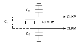
An external crystal is connected to the device pins. Figure 6-2 shows the crystal implementation.
 Figure 6-2 Crystal Implementation
The load capacitors, Cf1 and Cf2 in Figure 6-2, should be chosen such that Equation 1 is satisfied. CL in the equation is the load specified by the crystal manufacturer. All discrete components used to implement the oscillator circuit should be placed as close as possible to the associated oscillator CLKP and CLKM pins. Note that Cf1 and Cf2 include the parasitic capacitances due to PCB routing.

Table 6-10 lists the electrical characteristics of the clock crystal.
| NAME | DESCRIPTION | MIN | TYP | MAX | UNIT |
|---|---|---|---|---|---|
| fP | Parallel resonance crystal frequency | 40 | MHz | ||
| CL | Crystal load capacitance | 5 | 8 | 12 | pF |
| ESR | Crystal ESR | 50 | Ω | ||
| Temperature range | Expected temperature range of operation | –40 | 150 | °C | |
| Frequency tolerance | Crystal frequency tolerance(1)(2)(3) | –200 | 200 | ppm | |
| Drive level | 50 | 200 | µW |
A non-crystal oscillator can also be used as the clock reference source. In this case the signal is fed to the CLKP pin only and CLKM is grounded. Table 6-11 lists the electrical, AC timing, and phase noise requirements of the external oscillator input signal.
| PARAMETER | SPECIFICATION | UNIT | |||
|---|---|---|---|---|---|
| MIN | TYP | MAX | |||
| Input Clock: External AC-coupled sine wave or DC-coupled square wave Phase Noise referrenced to 40 MHz |
Frequency | 40 | MHz | ||
| AC-Amplitude | 700 | 1200 | mV (pp) | ||
| DC-VIL | 0.00 | 0.02 | V | ||
| DC-VIH | 1.40 | 1.95 | V | ||
| DC-trise/fall | 10 | ns | |||
| Phase Noise at 1 kHz | –132 | dBc/Hz | |||
| Phase Noise at 10 kHz | –143 | dBc/Hz | |||
| Phase Noise at 100 kHz | –152 | dBc/Hz | |||
| Phase Noise at 1 MHz | –153 | dBc/Hz | |||
| Duty Cycle | 35 | 65 | % | ||
| Freq Tolerance | –50 | 50 | ppm | ||