ZHCS488K October 2011 – December 2018 AM3351 , AM3352 , AM3354 , AM3356 , AM3357 , AM3358 , AM3359
PRODUCTION DATA.
- 1器件概述
- 2修订历史记录
- 3Device Comparison
- 4Terminal Configuration and Functions
-
5Specifications
- 5.1 Absolute Maximum Ratings
- 5.2 ESD Ratings
- 5.3 Power-On Hours (POH)
- 5.4 Operating Performance Points (OPPs)
- 5.5 Recommended Operating Conditions
- 5.6 Power Consumption Summary
- 5.7 DC Electrical Characteristics
- 5.8 Thermal Resistance Characteristics for ZCE and ZCZ Packages
- 5.9 External Capacitors
- 5.10 Touch Screen Controller and Analog-to-Digital Subsystem Electrical Parameters
-
6Power and Clocking
- 6.1 Power Supplies
- 6.2
Clock Specifications
- 6.2.1 Input Clock Specifications
- 6.2.2 Input Clock Requirements
- 6.2.3 Output Clock Specifications
- 6.2.4 Output Clock Characteristics
-
7Peripheral Information and Timings
- 7.1 Parameter Information
- 7.2 Recommended Clock and Control Signal Transition Behavior
- 7.3 OPP50 Support
- 7.4 Controller Area Network (CAN)
- 7.5 DMTimer
- 7.6
Ethernet Media Access Controller (EMAC) and Switch
- 7.6.1
EMAC and Switch Electrical Data and Timing
- Table 7-7 EMAC and Switch Timing Conditions
- 7.6.1.1 EMAC/Switch MDIO Electrical Data and Timing
- 7.6.1.2
EMAC and Switch MII Electrical Data and Timing
- Table 7-11 Timing Requirements for GMII[x]_RXCLK - MII Mode
- Table 7-12 Timing Requirements for GMII[x]_TXCLK - MII Mode
- Table 7-13 Timing Requirements for GMII[x]_RXD[3:0], GMII[x]_RXDV, and GMII[x]_RXER - MII Mode
- Table 7-14 Switching Characteristics for GMII[x]_TXD[3:0], and GMII[x]_TXEN - MII Mode
- 7.6.1.3 EMAC and Switch RMII Electrical Data and Timing
- 7.6.1.4
EMAC and Switch RGMII Electrical Data and Timing
- Table 7-18 Timing Requirements for RGMII[x]_RCLK - RGMII Mode
- Table 7-19 Timing Requirements for RGMII[x]_RD[3:0], and RGMII[x]_RCTL - RGMII Mode
- Table 7-20 Switching Characteristics for RGMII[x]_TCLK - RGMII Mode
- Table 7-21 Switching Characteristics for RGMII[x]_TD[3:0], and RGMII[x]_TCTL - RGMII Mode
- 7.6.1
EMAC and Switch Electrical Data and Timing
- 7.7
External Memory Interfaces
- 7.7.1 General-Purpose Memory Controller (GPMC)
- 7.7.2
mDDR(LPDDR), DDR2, DDR3, DDR3L Memory Interface
- 7.7.2.1
mDDR (LPDDR) Routing Guidelines
- 7.7.2.1.1 Board Designs
- 7.7.2.1.2 LPDDR Interface
- 7.7.2.1.3 LPDDR CK and ADDR_CTRL Routing
- 7.7.2.2
DDR2 Routing Guidelines
- 7.7.2.2.1 Board Designs
- 7.7.2.2.2
DDR2 Interface
- 7.7.2.2.2.1 DDR2 Interface Schematic
- 7.7.2.2.2.2 Compatible JEDEC DDR2 Devices
- 7.7.2.2.2.3 PCB Stackup
- 7.7.2.2.2.4 Placement
- 7.7.2.2.2.5 DDR2 Keepout Region
- 7.7.2.2.2.6 Bulk Bypass Capacitors
- 7.7.2.2.2.7 High-Speed (HS) Bypass Capacitors
- 7.7.2.2.2.8 Net Classes
- 7.7.2.2.2.9 DDR2 Signal Termination
- 7.7.2.2.2.10 DDR_VREF Routing
- 7.7.2.2.3 DDR2 CK and ADDR_CTRL Routing
- 7.7.2.3
DDR3 and DDR3L Routing Guidelines
- 7.7.2.3.1 Board Designs
- 7.7.2.3.2 DDR3 Device Combinations
- 7.7.2.3.3
DDR3 Interface
- 7.7.2.3.3.1 DDR3 Interface Schematic
- 7.7.2.3.3.2 Compatible JEDEC DDR3 Devices
- 7.7.2.3.3.3 PCB Stackup
- 7.7.2.3.3.4 Placement
- 7.7.2.3.3.5 DDR3 Keepout Region
- 7.7.2.3.3.6 Bulk Bypass Capacitors
- 7.7.2.3.3.7 High-Speed Bypass Capacitors
- 7.7.2.3.3.8 Net Classes
- 7.7.2.3.3.9 DDR3 Signal Termination
- 7.7.2.3.3.10 DDR_VREF Routing
- 7.7.2.3.3.11 VTT
- 7.7.2.3.4 DDR3 CK and ADDR_CTRL Topologies and Routing Definition
- 7.7.2.3.5 Data Topologies and Routing Definition
- 7.7.2.3.6 Routing Specification
- 7.7.2.1
mDDR (LPDDR) Routing Guidelines
- 7.8 I2C
- 7.9 JTAG Electrical Data and Timing
- 7.10 LCD Controller (LCDC)
- 7.11 Multichannel Audio Serial Port (McASP)
- 7.12 Multichannel Serial Port Interface (McSPI)
- 7.13
Multimedia Card (MMC) Interface
- 7.13.1
MMC Electrical Data and Timing
- Table 7-89 MMC Timing Conditions
- Table 7-90 Timing Requirements for MMC[x]_CMD and MMC[x]_DAT[7:0]
- Table 7-91 Switching Characteristics for MMC[x]_CLK
- Table 7-92 Switching Characteristics for MMC[x]_CMD and MMC[x]_DAT[7:0]—Standard Mode
- Table 7-93 Switching Characteristics for MMC[x]_CMD and MMC[x]_DAT[7:0]—High-Speed Mode
- 7.13.1
MMC Electrical Data and Timing
- 7.14
Programmable Real-Time Unit Subsystem and Industrial Communication Subsystem (PRU-ICSS)
- 7.14.1 Programmable Real-Time Unit (PRU-ICSS PRU)
- 7.14.2
PRU-ICSS EtherCAT (PRU-ICSS ECAT)
- Table 7-100 PRU-ICSS ECAT Timing Conditions
- 7.14.2.1
PRU-ICSS ECAT Electrical Data and Timing
- Table 7-101 PRU-ICSS ECAT Timing Requirements – Input Validated With LATCH_IN
- Table 7-102 PRU-ICSS ECAT Timing Requirements – Input Validated With SYNCx
- Table 7-103 PRU-ICSS ECAT Timing Requirements – Input Validated With Start of Frame (SOF)
- Table 7-104 PRU-ICSS ECAT Timing Requirements - LATCHx_IN
- Table 7-105 PRU-ICSS ECAT Switching Requirements - Digital I/Os
- 7.14.3 PRU-ICSS MII_RT and Switch
- 7.14.4 PRU-ICSS Universal Asynchronous Receiver Transmitter (PRU-ICSS UART)
- 7.15 Universal Asynchronous Receiver Transmitter (UART)
- 8Device and Documentation Support
- 9Mechanical, Packaging, and Orderable Information
封装选项
请参考 PDF 数据表获取器件具体的封装图。
机械数据 (封装 | 引脚)
- ZCZ|324
- ZCE|298
散热焊盘机械数据 (封装 | 引脚)
订购信息
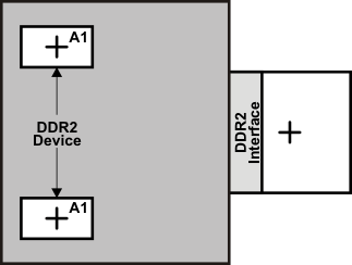
7.7.2.2.2.5 DDR2 Keepout Region
The region of the PCB used for the DDR2 circuitry must be isolated from other signals. The DDR2 keepout region is defined for this purpose and is shown in Figure 7-42. This region should encompass all DDR2 circuitry and the region size varies with component placement and DDR2 routing. Additional clearances required for the keepout region are shown in Table 7-49. Non-DDR2 signals must not be routed on the same signal layer as DDR2 signals within the DDR2 keepout region. Non-DDR2 signals may be routed in the region provided they are routed on layers separated from DDR2 signal layers by a ground layer. No breaks should be allowed in the reference ground or VDDS_DDR power plane in this region. In addition, the VDDS_DDR power plane should cover the entire keepout region.
