ZHCSDC3D June 2014 – September 2016 AM4372 , AM4376 , AM4377 , AM4378 , AM4379
PRODUCTION DATA.
- 1器件概述
- 2修订历史记录
- 3Device Comparison
-
4Terminal Configuration and Functions
- 4.1
Pin Diagrams
- ZDN Ball Map [Section Top Left - Top View]
- Table 4-1 ZDN Ball Map [Section Top Middle - Top View]
- Table 4-2 ZDN Ball Map [Section Top Right - Top View]
- Table 4-3 ZDN Ball Map [Section Middle Left - Top View]
- ZDN Ball Map [Section Middle Middle - Top View]
- ZDN Ball Map [Section Middle Right - Top View]
- Table 4-4 ZDN Ball Map [Section Bottom Left - Top View]
- Table 4-5 ZDN Ball Map [Section Bottom Middle - Top View]
- Table 4-6 ZDN Ball Map [Section Bottom Right - Top View]
- 4.2 Pin Attributes
- 4.3
Signal Descriptions
- 4.3.1 ADC Interfaces
- 4.3.2 CAN Interfaces
- 4.3.3 Camera (VPFE) Interfaces
- 4.3.4 Debug Subsystem Interface
- 4.3.5 Display Subsystem (DSS) Interface
- 4.3.6 Ethernet (GEMAC_CPSW) Interfaces
- 4.3.7 External Memory Interfaces
- 4.3.8 General Purpose IOs
- 4.3.9 HDQ Interface
- 4.3.10 I2C Interfaces
- 4.3.11 McASP Interfaces
- 4.3.12 Miscellaneous
- 4.3.13 PRU-ICSS0 Interface
- 4.3.14 PRU-ICSS1 Interface
- 4.3.15 QSPI Interface
- 4.3.16 RTC Subsystem Interface
- 4.3.17 Removable Media Interfaces
- 4.3.18 SPI Interfaces
- 4.3.19 Timer Interfaces
- 4.3.20 UART Interfaces
- 4.3.21 USB Interfaces
- 4.3.22 eCAP Interfaces
- 4.3.23 eHRPWM Interfaces
- 4.3.24 eQEP Interfaces
- 4.1
Pin Diagrams
-
5Specifications
- 5.1 Absolute Maximum Ratings
- 5.2 ESD Ratings
- 5.3 Power-On Hours (POH)
- 5.4 Operating Performance Points
- 5.5 Recommended Operating Conditions
- 5.6 Power Consumption Summary
- 5.7 DC Electrical Characteristics
- 5.8 ADC0: Touch Screen Controller and Analog-to-Digital Subsystem Electrical Parameters
- 5.9 ADC1: Analog-to-Digital Subsystem Electrical Parameters
- 5.10 VPP Specifications for One-Time Programmable (OTP) eFuses
- 5.11 Thermal Resistance Characteristics
- 5.12 External Capacitors
- 5.13
Timing and Switching Characteristics
- 5.13.1 Power Supply Sequencing
- 5.13.2
Clock
- 5.13.2.1 PLLs
- 5.13.2.2 Input Clock Specifications
- 5.13.2.3 Input Clock Requirements
- 5.13.2.4 Output Clock Specifications
- 5.13.2.5 Output Clock Characteristics
- 5.13.3 Timing Parameters and Board Routing Analysis
- 5.13.4 Recommended Clock and Control Signal Transition Behavior
- 5.13.5 Controller Area Network (CAN)
- 5.13.6 DMTimer
- 5.13.7
Ethernet Media Access Controller (EMAC) and Switch
- 5.13.7.1
Ethernet MAC and Switch Electrical Data and Timing
- Table 5-23 Ethernet MAC and Switch Timing Conditions
- 5.13.7.1.1 Ethernet MAC/Switch MDIO Electrical Data and Timing
- 5.13.7.1.2
Ethernet MAC and Switch MII Electrical Data and Timing
- Table 5-27 Timing Requirements for GMII[x]_RXCLK - MII Mode
- Table 5-28 Timing Requirements for GMII[x]_TXCLK - MII Mode
- Table 5-29 Timing Requirements for GMII[x]_RXD[3:0], GMII[x]_RXDV, and GMII[x]_RXER - MII Mode
- Table 5-30 Switching Characteristics for GMII[x]_TXD[3:0], and GMII[x]_TXEN - MII Mode
- 5.13.7.1.3 Ethernet MAC and Switch RMII Electrical Data and Timing
- 5.13.7.1.4
Ethernet MAC and Switch RGMII Electrical Data and Timing
- Table 5-34 Timing Requirements for RGMII[x]_RCLK - RGMII Mode
- Table 5-35 Timing Requirements for RGMII[x]_RD[3:0], and RGMII[x]_RCTL - RGMII Mode
- Table 5-36 Switching Characteristics for RGMII[x]_TCLK - RGMII Mode
- Table 5-37 Switching Characteristics for RGMII[x]_TD[3:0], and RGMII[x]_TCTL - RGMII Mode
- 5.13.7.1
Ethernet MAC and Switch Electrical Data and Timing
- 5.13.8
External Memory Interfaces
- 5.13.8.1 General-Purpose Memory Controller (GPMC)
- 5.13.8.2
Memory Interface
- 5.13.8.2.1
DDR3 and DDR3L Routing Guidelines
- 5.13.8.2.1.1 Board Designs
- 5.13.8.2.1.2 DDR3 Device Combinations
- 5.13.8.2.1.3
DDR3 Interface
- 5.13.8.2.1.3.1 DDR3 Interface Schematic
- 5.13.8.2.1.3.2 Compatible JEDEC DDR3 Devices
- 5.13.8.2.1.3.3 DDR3 PCB Stackup
- 5.13.8.2.1.3.4 DDR3 Placement
- 5.13.8.2.1.3.5 DDR3 Keepout Region
- 5.13.8.2.1.3.6 DDR3 Bulk Bypass Capacitors
- 5.13.8.2.1.3.7 DDR3 High-Speed Bypass Capacitors
- 5.13.8.2.1.3.8 DDR3 Net Classes
- 5.13.8.2.1.3.9 DDR3 Signal Termination
- 5.13.8.2.1.3.10 DDR3 DDR_VREF Routing
- 5.13.8.2.1.3.11 DDR3 VTT
- 5.13.8.2.1.4 DDR3 CK and ADDR_CTRL Topologies and Routing Definition
- 5.13.8.2.1.5 Data Topologies and Routing Definition
- 5.13.8.2.1.6 Routing Specification
- 5.13.8.2.2
LPDDR2 Routing Guidelines
- 5.13.8.2.2.1 LPDDR2 Board Designs
- 5.13.8.2.2.2 LPDDR2 Device Configurations
- 5.13.8.2.2.3
LPDDR2 Interface
- 5.13.8.2.2.3.1 LPDDR2 Interface Schematic
- 5.13.8.2.2.3.2 Compatible JEDEC LPDDR2 Devices
- 5.13.8.2.2.3.3 LPDDR2 PCB Stackup
- 5.13.8.2.2.3.4 LPDDR2 Placement
- 5.13.8.2.2.3.5 LPDDR2 Keepout Region
- 5.13.8.2.2.3.6 LPDDR2 Net Classes
- 5.13.8.2.2.3.7 LPDDR2 Signal Termination
- 5.13.8.2.2.3.8 LPDDR2 DDR_VREF Routing
- 5.13.8.2.2.4 Routing Specification
- 5.13.8.2.1
DDR3 and DDR3L Routing Guidelines
- 5.13.9 Display Subsystem (DSS)
- 5.13.10 Camera (VPFE)
- 5.13.11 Inter-Integrated Circuit (I2C)
- 5.13.12 Multichannel Audio Serial Port (McASP)
- 5.13.13 Multichannel Serial Port Interface (McSPI)
- 5.13.14 Quad Serial Port Interface (QSPI)
- 5.13.15 HDQ/1-Wire Interface (HDQ/1-Wire)
- 5.13.16
Programmable Real-Time Unit Subsystem and Industrial Communication Subsystem (PRU-ICSS)
- 5.13.16.1
Programmable Real-Time Unit (PRU-ICSS PRU)
- Table 5-100 PRU-ICSS PRU Timing Conditions
- 5.13.16.1.1 PRU-ICSS PRU Direct Input/Output Mode Electrical Data and Timing
- 5.13.16.1.2 PRU-ICSS PRU Parallel Capture Mode Electrical Data and Timing
- 5.13.16.1.3 PRU-ICSS PRU Shift Mode Electrical Data and Timing
- 5.13.16.1.4 PRU-ICSS Sigma Delta Electrical Data and Timing
- 5.13.16.1.5 PRU-ICSS ENDAT Electrical Data and Timing
- 5.13.16.2
PRU-ICSS EtherCAT (PRU-ICSS ECAT)
- Table 5-109 PRU-ICSS ECAT Timing Conditions
- 5.13.16.2.1
PRU-ICSS ECAT Electrical Data and Timing
- Table 5-110 PRU-ICSS ECAT Timing Requirements - Input Validated With LATCH_IN
- Table 5-111 PRU-ICSS ECAT Timing Requirements - Input Validated With SYNCx
- Table 5-112 PRU-ICSS ECAT Timing Requirements - Input Validated With Start of Frame (SOF)
- Table 5-113 PRU-ICSS ECAT Timing Requirements - LATCHx_IN
- Table 5-114 PRU-ICSS ECAT Switching Requirements - Digital IOs
- 5.13.16.3 PRU-ICSS MII_RT and Switch
- 5.13.16.4 PRU-ICSS Universal Asynchronous Receiver Transmitter (PRU-ICSS UART)
- 5.13.16.1
Programmable Real-Time Unit (PRU-ICSS PRU)
- 5.13.17
Multimedia Card (MMC) Interface
- 5.13.17.1
MMC Electrical Data and Timing
- Table 5-125 MMC Timing Conditions
- Table 5-126 Timing Requirements for MMC[0]_CMD and MMC[0]_DAT[7:0]
- Table 5-127 Timing Requirements for MMC[1/2]_CMD and MMC[1/2]_DAT[7:0]
- Table 5-128 Switching Characteristics for MMC[x]_CLK
- Table 5-129 Switching Characteristics for MMC[x]_CMD and MMC[x]_DAT[7:0]—HSPE=0
- Table 5-130 Switching Characteristics for MMC[x]_CMD and MMC[x]_DAT[7:0]—HSPE=1
- 5.13.17.1
MMC Electrical Data and Timing
- 5.13.18 Universal Asynchronous Receiver/Transmitter (UART)
- 5.14 Emulation and Debug
- 6Device and Documentation Support
- 7Mechanical, Packaging, and Orderable Information
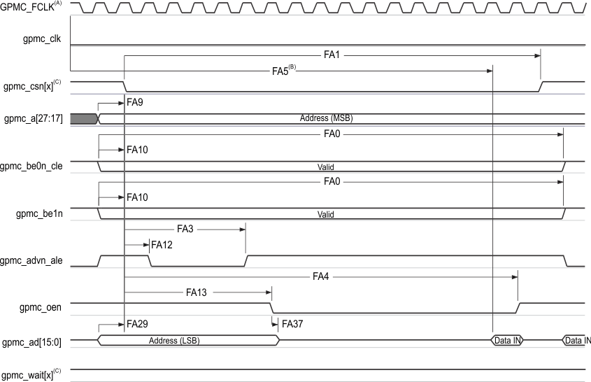
Table 5-44 GPMC and NOR Flash Switching Characteristics—Asynchronous Mode
| NO. | PARAMETER | OPP100 | OPP50 | UNIT | ||||
|---|---|---|---|---|---|---|---|---|
| MIN | MAX | MIN | MAX | |||||
| tR(d) | Rise time, output data gpmc_ad[15:0] | 2 | 2 | ns | ||||
| tF(d) | Fall time, output data gpmc_ad[15:0] | 2 | 2 | ns | ||||
| FA0 | tw(be[x]nV) | Pulse duration, output lower-byte enable and command latch enable gpmc_be0n_cle, output upper-byte enable gpmc_be1n valid time | Read | N(1) | N(1) | ns | ||
| Write | N(1) | N(1) | ||||||
| FA1 | tw(csnV) | Pulse duration, output chip select gpmc_csn[x](2) low | Read | A(3) | A(3) | ns | ||
| Write | A(3) | A(3) | ||||||
| FA3 | td(csnV-advnIV) | Delay time, output chip select gpmc_csn[x](2) valid to output address valid and address latch enable gpmc_advn_ale invalid | Read | B(4) – 0.2 | B(4) + 2.0 | B(4) – 0.2 | B(4) + 2.0 | ns |
| Write | B(4) – 0.2 | B(4) + 2.0 | B(4) – 0.2 | B(4) + 2.0 | ||||
| FA4 | td(csnV-oenIV) | Delay time, output chip select gpmc_csn[x](2) valid to output enable gpmc_oen invalid (Single read) | C(5) – 0.2 | C(5) + 2.0 | C(5) – 0.2 | C(5) + 2.0 | ns | |
| FA9 | td(aV-csnV) | Delay time, output address gpmc_a[27:1] valid to output chip select gpmc_csn[x](2) valid | J(6) – 0.2 | J(6) + 2.0 | J(6) – 0.2 | J(6) + 2.0 | ns | |
| FA10 | td(be[x]nV-csnV) | Delay time, output lower-byte enable and command latch enable gpmc_be0n_cle, output upper-byte enable gpmc_be1n valid to output chip select gpmc_csn[x](2) valid | J(6) – 0.2 | J(6) + 2.0 | J(6) – 0.2 | J(6) + 2.0 | ns | |
| FA12 | td(csnV-advnV) | Delay time, output chip select gpmc_csn[x](2) valid to output address valid and address latch enable gpmc_advn_ale valid | K(7) – 0.2 | K(7) + 2.0 | K(7) – 0.2 | K(7) + 2.0 | ns | |
| FA13 | td(csnV-oenV) | Delay time, output chip select gpmc_csn[x](2) valid to output enable gpmc_oen valid | L(8) – 0.2 | L(8) + 2.0 | L (8) – 0.2 | L(8) + 2.0 | ns | |
| FA16 | tw(aIV) | Pulse durationm output address gpmc_a[26:1] invalid between 2 successive read and write accesses | G(9) | G(9) | ns | |||
| FA18 | td(csnV-oenIV) | Delay time, output chip select gpmc_csn[x](2) valid to output enable gpmc_oen invalid (Burst read) | I(10) – 0.2 | I(10) + 2.0 | I(10) – 0.2 | I(10) + 2.0 | ns | |
| FA20 | tw(aV) | Pulse duration, output address gpmc_a[27:1] valid — 2nd, 3rd, and 4th accesses | D(11) | D(11) | ns | |||
| FA25 | td(csnV-wenV) | Delay time, output chip select gpmc_csn[x](2) valid to output write enable gpmc_wen valid | E(12) – 0.2 | E(12) + 2.0 | E(12) – 0.2 | E(12) + 2.0 | ns | |
| FA27 | td(csnV-wenIV) | Delay time, output chip select gpmc_csn[x](2) valid to output write enable gpmc_wen invalid | F(13) – 0.2 | F(13) + 2.0 | F(13) – 0.2 | F(13) + 2.0 | ns | |
| FA28 | td(wenV-dV) | Delay time, output write enable gpmc_ wen valid to output data gpmc_ad[15:0] valid | 2.8 | 5 | ns | |||
| FA29 | td(dV-csnV) | Delay time, output data gpmc_ad[15:0] valid to output chip select gpmc_csn[x](2) valid | J(6) – 0.2 | J(6) + 2.8 | J(6) – 0.2 | J(6) + 2.8 | ns | |
| FA37 | td(oenV-aIV) | Delay time, output enable gpmc_oen valid to output address gpmc_ad[15:0] phase end | 2.8 | 2.8 | ns | |||
- For single read: N = RdCycleTime × (TimeParaGranularity + 1) × GPMC_FCLK(14)
For single write: N = WrCycleTime × (TimeParaGranularity + 1) × GPMC_FCLK(14)
For burst read: N = (RdCycleTime + (n – 1) × PageBurstAccessTime) × (TimeParaGranularity + 1) × GPMC_FCLK(14)
For burst write: N = (WrCycleTime + (n – 1) × PageBurstAccessTime) × (TimeParaGranularity + 1) × GPMC_FCLK(14) - In gpmc_csn[x], x is equal to 0, 1, 2, 3, 4, 5, or 6.
- For single read: A = (CSRdOffTime – CSOnTime) × (TimeParaGranularity + 1) × GPMC_FCLK(14)
For single write: A = (CSWrOffTime – CSOnTime) × (TimeParaGranularity + 1) × GPMC_FCLK(14)
For burst read: A = (CSRdOffTime – CSOnTime + (n – 1) × PageBurstAccessTime) × (TimeParaGranularity + 1) × GPMC_FCLK(14)
For burst write: A = (CSWrOffTime – CSOnTime + (n – 1) × PageBurstAccessTime) × (TimeParaGranularity + 1) × GPMC_FCLK(14)
with n being the page burst access number - For reading: B = ((ADVRdOffTime – CSOnTime) × (TimeParaGranularity + 1) + 0.5 × (ADVExtraDelay – CSExtraDelay)) × GPMC_FCLK(14)
For writing: B = ((ADVWrOffTime – CSOnTime) × (TimeParaGranularity + 1) + 0.5 × (ADVExtraDelay – CSExtraDelay)) × GPMC_FCLK(14) - C = ((OEOffTime – CSOnTime) × (TimeParaGranularity + 1) + 0.5 × (OEExtraDelay – CSExtraDelay)) × GPMC_FCLK(14)
- J = (CSOnTime × (TimeParaGranularity + 1) + 0.5 × CSExtraDelay) × GPMC_FCLK(14)
- K = ((ADVOnTime – CSOnTime) × (TimeParaGranularity + 1) + 0.5 × (ADVExtraDelay – CSExtraDelay)) × GPMC_FCLK(14)
- L = ((OEOnTime – CSOnTime) × (TimeParaGranularity + 1) + 0.5 × (OEExtraDelay – CSExtraDelay)) × GPMC_FCLK(14)
- G = Cycle2CycleDelay × GPMC_FCLK(14)
- I = ((OEOffTime + (n – 1) × PageBurstAccessTime – CSOnTime) × (TimeParaGranularity + 1) + 0.5 × (OEExtraDelay – CSExtraDelay)) × GPMC_FCLK(14)
- D = PageBurstAccessTime × (TimeParaGranularity + 1) × GPMC_FCLK(14)
- E = ((WEOnTime – CSOnTime) × (TimeParaGranularity + 1) + 0.5 × (WEExtraDelay – CSExtraDelay)) × GPMC_FCLK(14)
- F = ((WEOffTime – CSOnTime) × (TimeParaGranularity + 1) + 0.5 × (WEExtraDelay – CSExtraDelay)) × GPMC_FCLK(14)
- GPMC_FCLK is general-purpose memory controller internal functional clock period in ns.
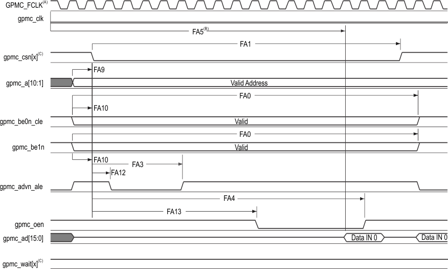
A. GPMC_FCLK is an internal clock (GPMC functional clock) not provided externally.
B. FA5 parameter illustrates amount of time required to internally sample input data. It is expressed in number of GPMC functional clock cycles. From start of read cycle and after FA5 functional clock cycles, input data will be internally sampled by active functional clock edge. FA5 value must be stored inside AccessTime register bits field.
C. In gpmc_csn[x], x is equal to 0, 1, 2, 3, 4, 5, or 6. In gpmc_wait[x], x is equal to 0 or 1.
Figure 5-38 GPMC and NOR Flash—Asynchronous Read—Single Word
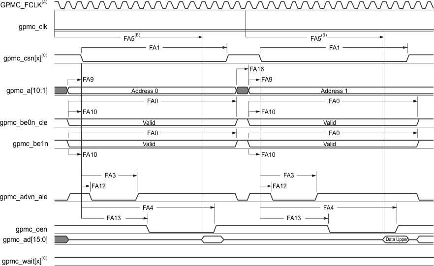
A. GPMC_FCLK is an internal clock (GPMC functional clock) not provided externally.
B. FA5 parameter illustrates amount of time required to internally sample input data. It is expressed in number of GPMC functional clock cycles. From start of read cycle and after FA5 functional clock cycles, input data will be internally sampled by active functional clock edge. FA5 value must be stored inside AccessTime register bits field.
C. In gpmc_csn[x], x is equal to 0, 1, 2, 3, 4, 5, or 6. In gpmc_wait[x], x is equal to 0 or 1.
Figure 5-39 GPMC and NOR Flash—Asynchronous Read—32-Bit
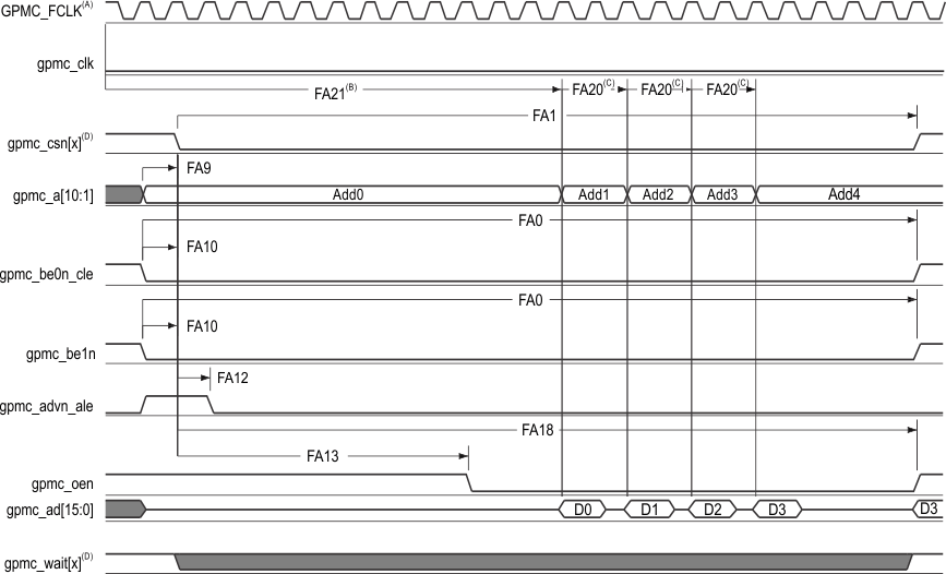
A. GPMC_FCLK is an internal clock (GPMC functional clock) not provided externally.
B. FA21 parameter illustrates amount of time required to internally sample first input page data. It is expressed in number of GPMC functional clock cycles. From start of read cycle and after FA21 functional clock cycles, first input page data will be internally sampled by active functional clock edge. FA21 calculation must be stored inside AccessTime register bits field.
C. FA20 parameter illustrates amount of time required to internally sample successive input page data. It is expressed in number of GPMC functional clock cycles. After each access to input page data, next input page data will be internally sampled by active functional clock edge after FA20 functional clock cycles. FA20 is also the duration of address phases for successive input page data (excluding first input page data). FA20 value must be stored in PageBurstAccessTime register bits field.
D. In gpmc_csn[x], x is equal to 0, 1, 2, 3, 4, 5, or 6. In gpmc_wait[x], x is equal to 0 or 1.
Figure 5-40 GPMC and NOR Flash—Asynchronous Read—Page Mode 4x16-Bit
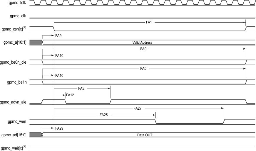
A. In gpmc_csn[x], x is equal to 0, 1, 2, 3, 4, 5, or 6. In gpmc_wait[x], x is equal to 0 or 1.
Figure 5-41 GPMC and NOR Flash—Asynchronous Write—Single Word
A. GPMC_FCLK is an internal clock (GPMC functional clock) not provided externally.
B. FA5 parameter illustrates amount of time required to internally sample input data. It is expressed in number of GPMC functional clock cycles. From start of read cycle and after FA5 functional clock cycles, input data will be internally sampled by active functional clock edge. FA5 value must be stored inside AccessTime register bits field.
C. In gpmc_csn[x], x is equal to 0, 1, 2, 3, 4, 5, or 6. In gpmc_wait[x], x is equal to 0 or 1.
Figure 5-42 GPMC and Multiplexed NOR Flash—Asynchronous Read—Single Word
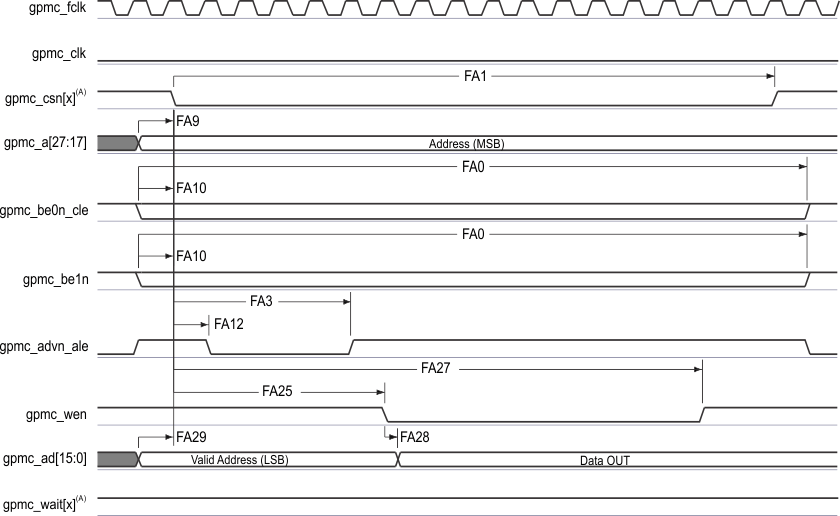
A. In gpmc_csn[x], x is equal to 0, 1, 2, 3, 4, 5, or 6. In gpmc_wait[x], x is equal to 0 or 1.
Figure 5-43 GPMC and Multiplexed NOR Flash—Asynchronous Write—Single Word